• 文献检索
  • 文档翻译
  • 深度研究
  • 学术资讯
  • Suppr Zotero 插件Zotero 插件
  • 邀请有礼
  • 套餐&价格
  • 历史记录
应用&插件
Suppr Zotero 插件Zotero 插件浏览器插件Mac 客户端Windows 客户端微信小程序
定价
高级版会员购买积分包购买API积分包
服务
文献检索文档翻译深度研究API 文档MCP 服务
关于我们
关于 Suppr公司介绍联系我们用户协议隐私条款
关注我们

Suppr 超能文献

核心技术专利:CN118964589B侵权必究
粤ICP备2023148730 号-1Suppr @ 2026

文献检索

告别复杂PubMed语法,用中文像聊天一样搜索,搜遍4000万医学文献。AI智能推荐,让科研检索更轻松。

立即免费搜索

文件翻译

保留排版,准确专业,支持PDF/Word/PPT等文件格式,支持 12+语言互译。

免费翻译文档

深度研究

AI帮你快速写综述,25分钟生成高质量综述,智能提取关键信息,辅助科研写作。

立即免费体验

溶液法制备的氧化锌薄膜的形貌对薄膜晶体管电学特性的影响

Morphological Influence of Solution-Processed Zinc Oxide Films on Electrical Characteristics of Thin-Film Transistors.

作者信息

Lee Hyeonju, Zhang Xue, Hwang Jaeeun, Park Jaehoon

机构信息

Department of Electronic Engineering, Hallym University, Chuncheon 24252, Korea.

Department of Advanced Materials Engineering for Information & Electronics, Kyung Hee University, Yongin 17104, Korea.

出版信息

Materials (Basel). 2016 Oct 19;9(10):851. doi: 10.3390/ma9100851.

DOI:10.3390/ma9100851
PMID:28773973
原文链接:https://pmc.ncbi.nlm.nih.gov/articles/PMC5456589/
Abstract

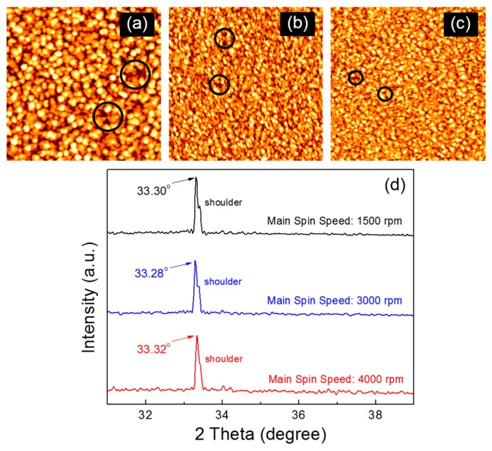
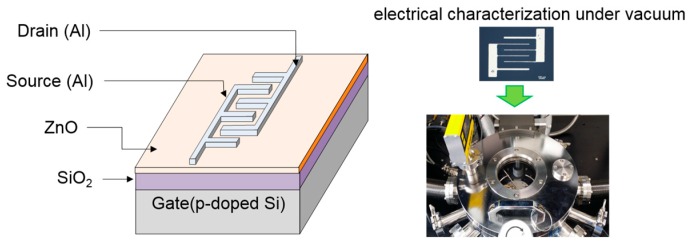
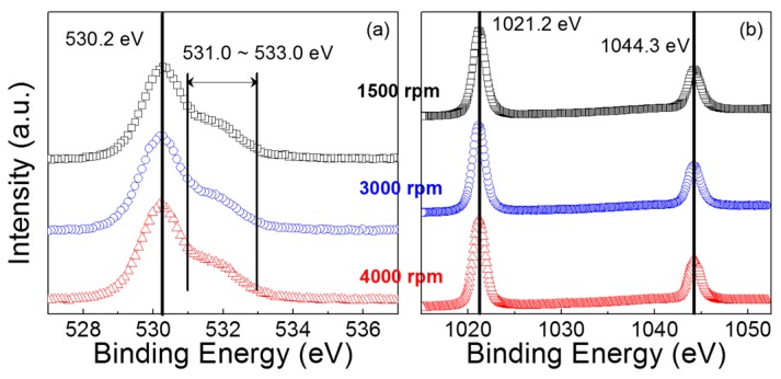
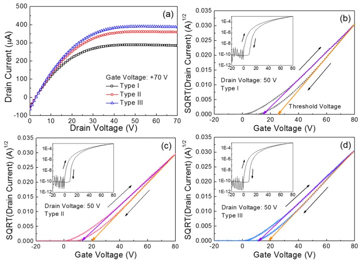
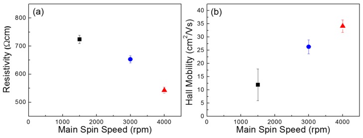
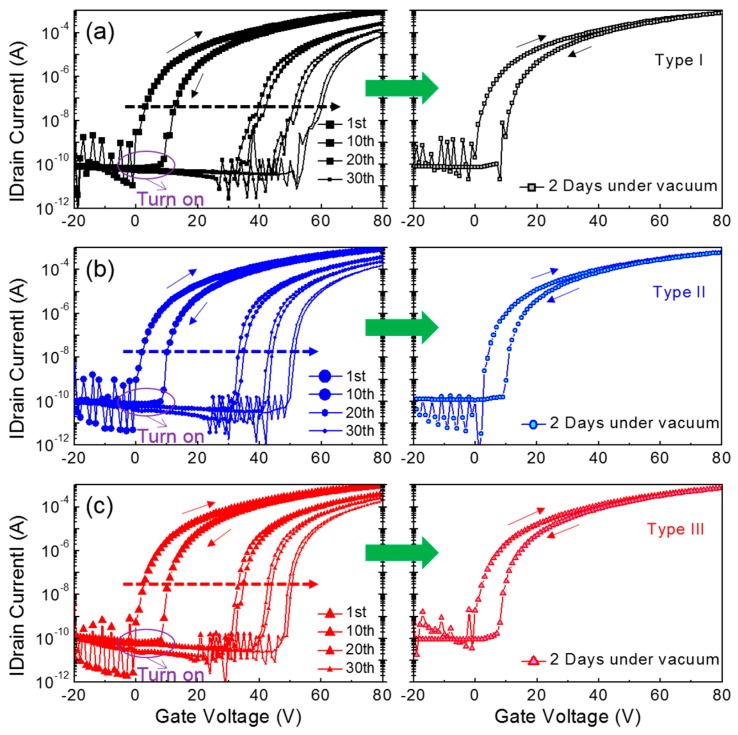
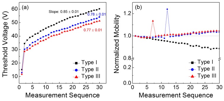
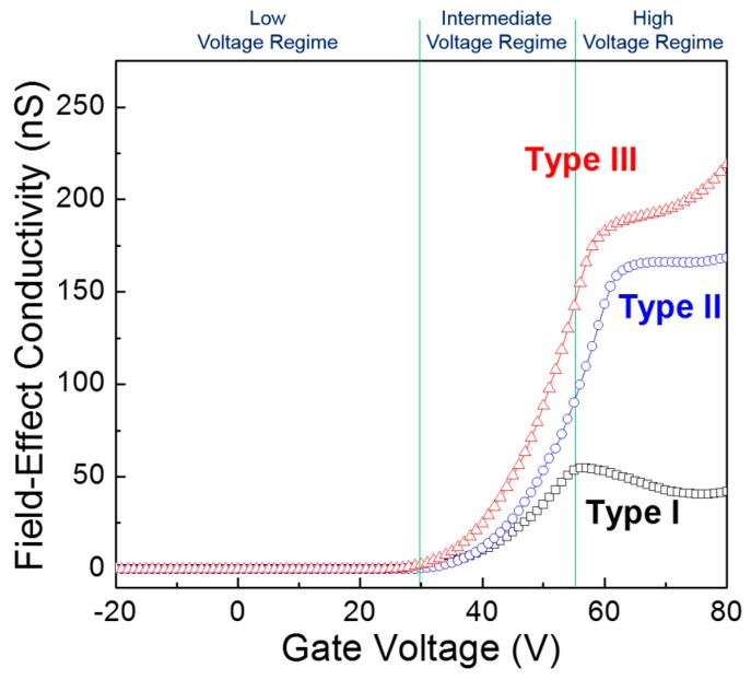
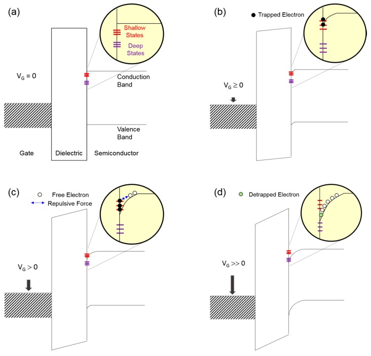
We report on the morphological influence of solution-processed zinc oxide (ZnO) semiconductor films on the electrical characteristics of ZnO thin-film transistors (TFTs). Different film morphologies were produced by controlling the spin-coating condition of a precursor solution, and the ZnO films were analyzed using atomic force microscopy, X-ray diffraction, X-ray photoemission spectroscopy, and Hall measurement. It is shown that ZnO TFTs have a superior performance in terms of the threshold voltage and field-effect mobility, when ZnO crystallites are more densely packed in the film. This is attributed to lower electrical resistivity and higher Hall mobility in a densely packed ZnO film. In the results of consecutive TFT operations, a positive shift in the threshold voltage occurred irrespective of the film morphology, but the morphological influence on the variation in the field-effect mobility was evident. The field-effect mobility in TFTs having a densely packed ZnO film increased continuously during consecutive TFT operations, which is in contrast to the mobility decrease observed in the less packed case. An analysis of the field-effect conductivities ascribes these results to the difference in energetic traps, which originate from structural defects in the ZnO films. Consequently, the morphological influence of solution-processed ZnO films on the TFT performance can be understood through the packing property of ZnO crystallites.

摘要

我们报道了溶液法制备的氧化锌(ZnO)半导体薄膜对ZnO薄膜晶体管(TFT)电学特性的形态学影响。通过控制前驱体溶液的旋涂条件制备了不同的薄膜形态,并使用原子力显微镜、X射线衍射、X射线光电子能谱和霍尔测量对ZnO薄膜进行了分析。结果表明,当ZnO微晶在薄膜中更紧密堆积时,ZnO TFT在阈值电压和场效应迁移率方面具有优异的性能。这归因于紧密堆积的ZnO薄膜中较低的电阻率和较高的霍尔迁移率。在连续的TFT操作结果中,无论薄膜形态如何,阈值电压都会出现正向偏移,但形态对场效应迁移率变化的影响是明显的。具有紧密堆积ZnO薄膜的TFT中的场效应迁移率在连续的TFT操作过程中持续增加,这与在堆积较少情况下观察到的迁移率降低形成对比。对场效应电导率的分析将这些结果归因于能量陷阱的差异,这些陷阱源于ZnO薄膜中的结构缺陷。因此,通过ZnO微晶的堆积特性可以理解溶液法制备的ZnO薄膜对TFT性能的形态学影响。

https://cdn.ncbi.nlm.nih.gov/pmc/blobs/c82c/5456589/24ac403c7115/materials-09-00851-g010.jpg
https://cdn.ncbi.nlm.nih.gov/pmc/blobs/c82c/5456589/dfc520995e54/materials-09-00851-g001.jpg
https://cdn.ncbi.nlm.nih.gov/pmc/blobs/c82c/5456589/7fb20e79a21e/materials-09-00851-g002.jpg
https://cdn.ncbi.nlm.nih.gov/pmc/blobs/c82c/5456589/ed4dc1e90870/materials-09-00851-g003.jpg
https://cdn.ncbi.nlm.nih.gov/pmc/blobs/c82c/5456589/a567a51ec112/materials-09-00851-g004.jpg
https://cdn.ncbi.nlm.nih.gov/pmc/blobs/c82c/5456589/92351f59a566/materials-09-00851-g005.jpg
https://cdn.ncbi.nlm.nih.gov/pmc/blobs/c82c/5456589/7fd4a54bd054/materials-09-00851-g006.jpg
https://cdn.ncbi.nlm.nih.gov/pmc/blobs/c82c/5456589/9ac5d2e7fd3b/materials-09-00851-g007.jpg
https://cdn.ncbi.nlm.nih.gov/pmc/blobs/c82c/5456589/bdc0619d4f38/materials-09-00851-g008.jpg
https://cdn.ncbi.nlm.nih.gov/pmc/blobs/c82c/5456589/b46d8d17ed57/materials-09-00851-g009.jpg
https://cdn.ncbi.nlm.nih.gov/pmc/blobs/c82c/5456589/24ac403c7115/materials-09-00851-g010.jpg

相似文献

1
Morphological Influence of Solution-Processed Zinc Oxide Films on Electrical Characteristics of Thin-Film Transistors.溶液法制备的氧化锌薄膜的形貌对薄膜晶体管电学特性的影响
Materials (Basel). 2016 Oct 19;9(10):851. doi: 10.3390/ma9100851.
2
Low-Concentration Indium Doping in Solution-Processed Zinc Oxide Films for Thin-Film Transistors.用于薄膜晶体管的溶液法氧化锌薄膜中的低浓度铟掺杂
Materials (Basel). 2017 Jul 31;10(8):880. doi: 10.3390/ma10080880.
3
Investigation of the Electrical Characteristics of Bilayer ZnO/In₂O₃ Thin-Film Transistors Fabricated by Solution Processing.溶液法制备双层ZnO/In₂O₃薄膜晶体管的电学特性研究
Materials (Basel). 2018 Oct 26;11(11):2103. doi: 10.3390/ma11112103.
4
Effects of Post-UV/Ozone Treatment on Electrical Characteristics of Solution-Processed Copper Oxide Thin-Film Transistors.紫外/臭氧后处理对溶液法制备的氧化铜薄膜晶体管电学特性的影响
Nanomaterials (Basel). 2023 Feb 24;13(5):854. doi: 10.3390/nano13050854.
5
Lanthanum Doping in Zinc Oxide for Highly Reliable Thin-Film Transistors on Flexible Substrates by Spray Pyrolysis.通过喷雾热解法在氧化锌中掺杂镧用于在柔性基板上制备高可靠性薄膜晶体管
ACS Appl Mater Interfaces. 2020 Aug 5;12(31):35164-35174. doi: 10.1021/acsami.0c05151. Epub 2020 Jul 22.
6
Solution-Processed Gallium-Tin-Based Oxide Semiconductors for Thin-Film Transistors.用于薄膜晶体管的溶液法制备的镓锡基氧化物半导体
Materials (Basel). 2017 Dec 28;11(1):46. doi: 10.3390/ma11010046.
7
Schottky barrier thin film transistors using solution-processed n-ZnO.采用溶液法制备的 n-ZnO 的肖特基势垒薄膜晶体管。
ACS Appl Mater Interfaces. 2012 Mar;4(3):1423-8. doi: 10.1021/am201656h. Epub 2012 Mar 12.
8
Investigation on Atomic Bonding Structure of Solution-Processed Indium-Zinc-Oxide Semiconductors According to Doped Indium Content and Its Effects on the Transistor Performance.基于掺杂铟含量的溶液法制备铟锌氧化物半导体原子键合结构及其对晶体管性能影响的研究
Materials (Basel). 2022 Sep 29;15(19):6763. doi: 10.3390/ma15196763.
9
Photo-Patternable ZnO Thin Films Based on Cross-Linked Zinc Acrylate for Organic/Inorganic Hybrid Complementary Inverters.基于交联丙烯酸锌的光图案化 ZnO 薄膜在有机/无机杂化互补反相器中的应用。
ACS Appl Mater Interfaces. 2016 Mar 2;8(8):5499-508. doi: 10.1021/acsami.6b00259. Epub 2016 Feb 16.
10
Dual-Functional Superoxide Precursor To Improve the Electrical Characteristics of Oxide Thin Film Transistors.双功能超氧化物前体改善氧化物薄膜晶体管的电性能。
ACS Appl Mater Interfaces. 2018 Dec 26;10(51):44554-44560. doi: 10.1021/acsami.8b16961. Epub 2018 Dec 14.

引用本文的文献

1
Effects of Iodine Doping on Electrical Characteristics of Solution-Processed Copper Oxide Thin-Film Transistors.碘掺杂对溶液法制备的氧化铜薄膜晶体管电学特性的影响
Materials (Basel). 2021 Oct 15;14(20):6118. doi: 10.3390/ma14206118.
2
Elemental and Thermochemical Analyses of Materials after Electrical Discharge Machining in Water: Focus on Ni and Zn.水中放电加工后材料的元素与热化学分析:聚焦于镍和锌
Materials (Basel). 2021 Jun 9;14(12):3189. doi: 10.3390/ma14123189.
3
Highly Transparent and Surface-Plasmon-Enhanced Visible-Photodetector Based on Zinc Oxide Thin-Film Transistors with Heterojunction Structure.

本文引用的文献

1
Improved photocatalytic activity in RuO2-ZnO nanoparticulate heterostructures due to inhomogeneous space charge effects.由于非均匀空间电荷效应,RuO2-ZnO纳米颗粒异质结构中的光催化活性得到改善。
Phys Chem Chem Phys. 2015 Feb 21;17(7):5090-102. doi: 10.1039/c4cp04780j.
2
Multifunctional CuO nanowire devices: p-type field effect transistors and CO gas sensors.多功能氧化铜纳米线器件:p型场效应晶体管和一氧化碳气体传感器。
Nanotechnology. 2009 Feb 25;20(8):085203. doi: 10.1088/0957-4484/20/8/085203. Epub 2009 Feb 2.
3
Dopability, intrinsic conductivity, and nonstoichiometry of transparent conducting oxides.
基于具有异质结结构的氧化锌薄膜晶体管的高透明且表面等离子体增强型可见光电探测器。
Materials (Basel). 2019 Nov 5;12(21):3639. doi: 10.3390/ma12213639.
4
Investigation of the Electrical Characteristics of Bilayer ZnO/In₂O₃ Thin-Film Transistors Fabricated by Solution Processing.溶液法制备双层ZnO/In₂O₃薄膜晶体管的电学特性研究
Materials (Basel). 2018 Oct 26;11(11):2103. doi: 10.3390/ma11112103.
5
Solution-Processed Gallium-Tin-Based Oxide Semiconductors for Thin-Film Transistors.用于薄膜晶体管的溶液法制备的镓锡基氧化物半导体
Materials (Basel). 2017 Dec 28;11(1):46. doi: 10.3390/ma11010046.
6
Low-Concentration Indium Doping in Solution-Processed Zinc Oxide Films for Thin-Film Transistors.用于薄膜晶体管的溶液法氧化锌薄膜中的低浓度铟掺杂
Materials (Basel). 2017 Jul 31;10(8):880. doi: 10.3390/ma10080880.
透明导电氧化物的可掺杂性、本征导电性和非化学计量比。
Phys Rev Lett. 2007 Jan 26;98(4):045501. doi: 10.1103/PhysRevLett.98.045501. Epub 2007 Jan 23.