Riazimehr Sarah, Kataria Satender, Bornemann Rainer, Haring Bolívar Peter, Ruiz Francisco Javier Garcia, Engström Olof, Godoy Andres, Lemme Max C
University of Siegen, School of Science and Technology, Department of Electrical Engineering and Computer Science, Hölderlinstr. 3, 57076 Siegen, Germany.
RWTH Aachen University, Faculty of Electrical Engineering and Information Technology, Chair for Electronic Devices, Otto-Blumenthal-Str. 25, 52074 Aachen, Germany.
ACS Photonics. 2017 Jun 21;4(6):1506-1514. doi: 10.1021/acsphotonics.7b00285. Epub 2017 May 30.
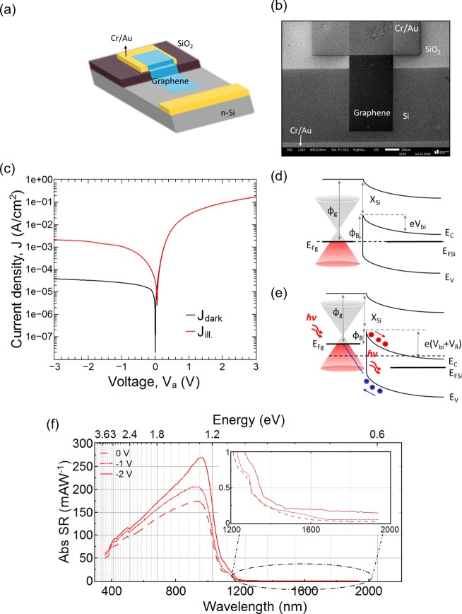
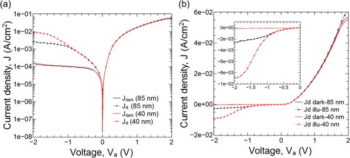
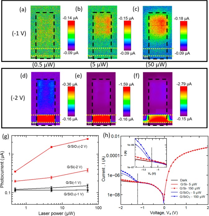
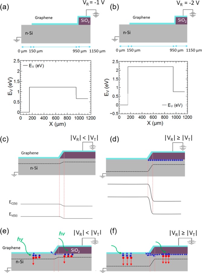
Graphene/silicon (G/Si) heterojunction based devices have been demonstrated as high responsivity photodetectors that are potentially compatible with semiconductor technology. Such G/Si Schottky junction diodes are typically in parallel with gated G/silicon dioxide (SiO)/Si areas, where the graphene is contacted. Here, we utilize scanning photocurrent measurements to investigate the spatial distribution and explain the physical origin of photocurrent generation in these devices. We observe distinctly higher photocurrents underneath the isolating region of graphene on SiO adjacent to the Schottky junction of G/Si. A certain threshold voltage () is required before this can be observed, and its origins are similar to that of the threshold voltage in metal oxide semiconductor field effect transistors. A physical model serves to explain the large photocurrents underneath SiO by the formation of an inversion layer in Si. Our findings contribute to a basic understanding of graphene/semiconductor hybrid devices which, in turn, can help in designing efficient optoelectronic devices and systems based on such 2D/3D heterojunctions.
基于石墨烯/硅(G/Si)异质结的器件已被证明是具有高响应度的光电探测器,有可能与半导体技术兼容。这种G/Si肖特基结二极管通常与石墨烯接触的栅控G/二氧化硅(SiO)/Si区域并联。在这里,我们利用扫描光电流测量来研究这些器件中光电流产生的空间分布并解释其物理起源。我们观察到,在与G/Si肖特基结相邻的SiO上石墨烯的隔离区域下方,光电流明显更高。在观察到这种情况之前需要一定的阈值电压(),其起源与金属氧化物半导体场效应晶体管中的阈值电压类似。一个物理模型用于解释通过在Si中形成反型层而在SiO下方产生的大光电流。我们的发现有助于对石墨烯/半导体混合器件有基本的了解,这反过来又有助于设计基于此类二维/三维异质结的高效光电器件和系统。