Dutta Neilanjan, Mirza Iftekhar O, Shi Shouyuan, Prather Dennis W
Department of Electrical and Computer Engineering, University of Delaware, Newark, DE 19716, USA.
Materials (Basel). 2010 Dec 15;3(12):5283-5292. doi: 10.3390/ma3125283.
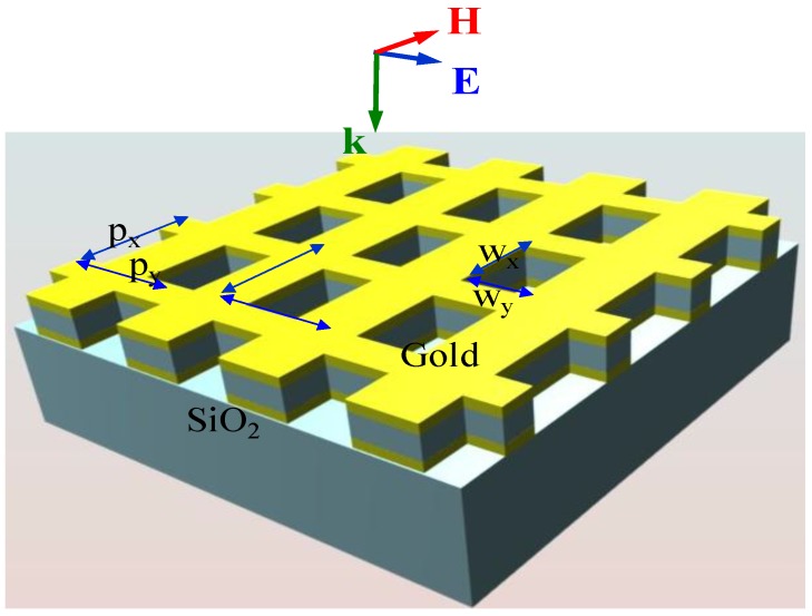
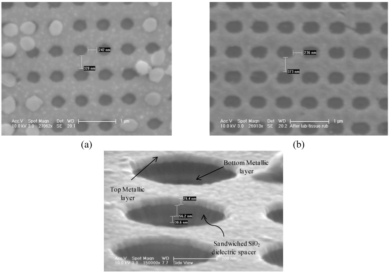
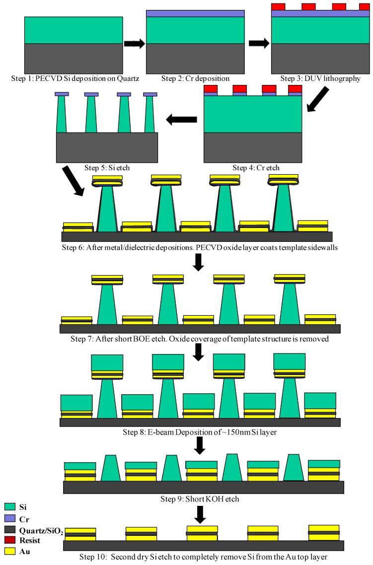
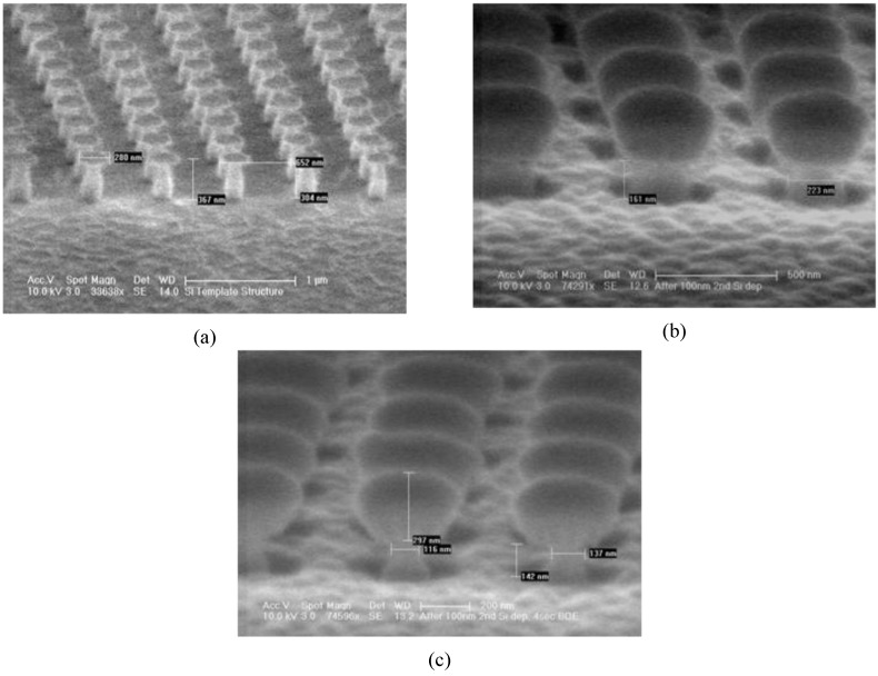
In this paper, we demonstrate a fabrication process for large area (2 mm × 2 mm) fishnet metamaterial structures for near IR wavelengths. This process involves: (a) defining a sacrificial Si template structure onto a quartz wafer using deep-UV lithography and a dry etching process (b) deposition of a stack of Au-SiO₂-Au layers and (c) a 'lift-off' process which removes the sacrificial template structure to yield the fishnet structure. The fabrication steps in this process are compatible with today's CMOS technology making it eminently well suited for batch fabrication. Also, depending on area of the exposure mask available for patterning the template structure, this fabrication process can potentially lead to optical metamaterials spanning across wafer-size areas.
在本文中,我们展示了一种用于近红外波长的大面积(2毫米×2毫米)渔网超材料结构的制造工艺。该工艺包括:(a)使用深紫外光刻和干法蚀刻工艺在石英晶片上定义一个牺牲性硅模板结构;(b)沉积一层Au-SiO₂-Au层;(c)通过“剥离”工艺去除牺牲性模板结构,从而得到渔网结构。此工艺中的制造步骤与当今的CMOS技术兼容,使其非常适合批量制造。此外,根据可用于对模板结构进行图案化的曝光掩膜面积,这种制造工艺有可能制造出跨越整个晶圆尺寸区域的光学超材料。