Department of Electrical Engineering, Stanford University, Stanford, CA, 94305, USA.
Hefei National Laboratory for Physical Sciences at the Microscale and Department of Modern Physics, University of Science and Technology of China, Hefei, Anhui, 230026, China.
Nat Commun. 2017 Sep 20;8(1):628. doi: 10.1038/s41467-017-00733-y.
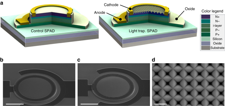
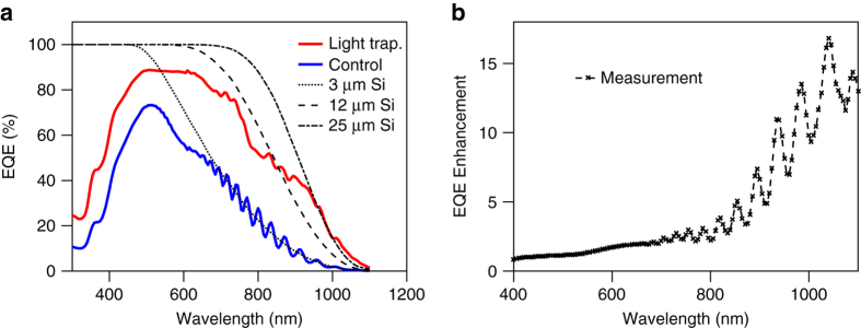
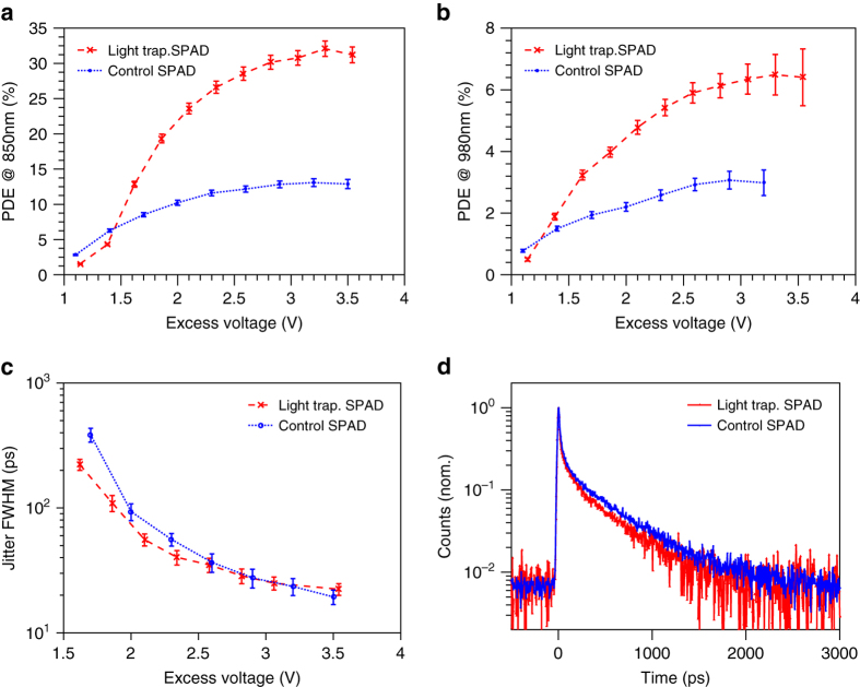
Silicon single-photon avalanche detectors are becoming increasingly significant in research and in practical applications due to their high signal-to-noise ratio, complementary metal oxide semiconductor compatibility, room temperature operation, and cost-effectiveness. However, there is a trade-off in current silicon single-photon avalanche detectors, especially in the near infrared regime. Thick-junction devices have decent photon detection efficiency but poor timing jitter, while thin-junction devices have good timing jitter but poor efficiency. Here, we demonstrate a light-trapping, thin-junction Si single-photon avalanche diode that breaks this trade-off, by diffracting the incident photons into the horizontal waveguide mode, thus significantly increasing the absorption length. The photon detection efficiency has a 2.5-fold improvement in the near infrared regime, while the timing jitter remains 25 ps. The result provides a practical and complementary metal oxide semiconductor compatible method to improve the performance of single-photon avalanche detectors, image sensor arrays, and silicon photomultipliers over a broad spectral range.The performance of silicon single-photon avalanche detectors is currently limited by the trade-off between photon detection efficiency and timing jitter. Here, the authors demonstrate how a CMOS-compatible, nanostructured, thin junction structure can make use of tailored light trapping to break this trade-off.
硅单光子雪崩探测器由于其高信噪比、与互补金属氧化物半导体的兼容性、室温工作以及成本效益,在研究和实际应用中变得越来越重要。然而,目前的硅单光子雪崩探测器存在权衡,特别是在近红外区域。厚结器件具有良好的光子探测效率,但定时抖动较差,而薄结器件具有良好的定时抖动,但效率较低。在这里,我们展示了一种光捕获的、薄结的 Si 单光子雪崩二极管,它通过将入射光子衍射到水平波导模式,从而显著增加吸收长度,打破了这种权衡。在近红外区域,光子探测效率提高了 2.5 倍,而定时抖动仍然保持在 25 ps。该结果提供了一种实用的、与互补金属氧化物半导体兼容的方法,可以在宽光谱范围内提高单光子雪崩探测器、图像传感器阵列和硅光电倍增器的性能。硅单光子雪崩探测器的性能目前受到光子探测效率和定时抖动之间权衡的限制。在这里,作者展示了如何利用结构精巧的光捕获,利用 CMOS 兼容的纳米结构薄结结构来打破这种权衡。