Nanophotonics Research Division, CAS Center for Excellence in Nanoscience, National Center for Nanoscience and Technology, Beijing, 100190, China.
Department of Physics, Stony Brook University, Stony Brook, NY, 11794, USA.
Nat Commun. 2017 Nov 13;8(1):1471. doi: 10.1038/s41467-017-01580-7.
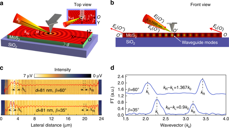
Most van der Waals crystals present highly anisotropic optical responses due to their strong in-plane covalent bonding and weak out-of-plane interactions. However, the determination of the polarization-dependent dielectric constants of van der Waals crystals remains a nontrivial task, since the size and dimension of the samples are often below or close to the diffraction limit of the probe light. In this work, we apply an optical nano-imaging technique to determine the anisotropic dielectric constants in representative van der Waals crystals. Through the study of both ordinary and extraordinary waveguide modes in real space, we are able to quantitatively determine the full dielectric tensors of nanometer-thin molybdenum disulfide and hexagonal boron nitride microcrystals, the most-promising van der Waals semiconductor and dielectric. Unlike traditional reflection-based methods, our measurements are reliable below the length scale of the free-space wavelength and reveal a universal route for characterizing low-dimensional crystals with high anisotropies.
大多数范德华晶体由于其强烈的面内共价键和较弱的面外相互作用而呈现出各向异性的光学响应。然而,由于样品的尺寸和维度通常低于或接近探针光的衍射极限,因此确定范德华晶体的偏振相关介电常数仍然是一项具有挑战性的任务。在这项工作中,我们应用一种光学纳米成像技术来确定代表性范德华晶体的各向异性介电常数。通过对真空中寻常波和非寻常波导模式的研究,我们能够定量地确定纳米级二硫化钼和六方氮化硼微晶体的完整介电张量,这两种晶体是最有前途的范德华半导体和介电体。与传统的基于反射的方法不同,我们的测量在自由空间波长的长度尺度以下是可靠的,并且为具有高各向异性的低维晶体的表征提供了一种通用方法。