Nazir Ghazanfar, Khan Muhammad Farooq, Aftab Sikandar, Afzal Amir Muhammad, Dastgeer Ghulam, Rehman Malik Abdul, Seo Yongho, Eom Jonghwa
Department of Physics & Astronomy and Graphene Research Institute, Sejong University, Seoul 05006, Korea.
Department of Nanotechnology & Advanced Materials Engineering, Sejong University, Seoul 05006, Korea.
Nanomaterials (Basel). 2017 Dec 28;8(1):14. doi: 10.3390/nano8010014.
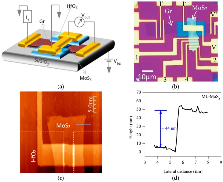
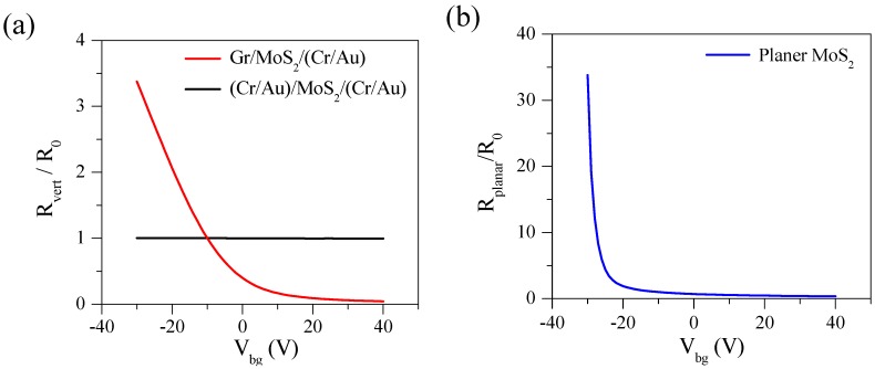
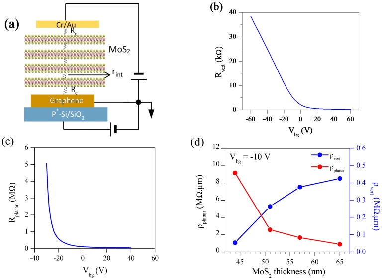
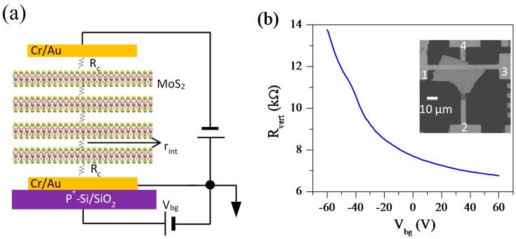
Two-dimensional materials based vertical field-effect transistors have been widely studied due to their useful applications in industry. In the present study, we fabricate graphene/MoS₂/(Cr/Au) vertical transistor based on the mechanical exfoliation and dry transfer method. Since the bottom electrode was made of monolayer graphene (Gr), the electrical transport in our Gr/MoS₂/(Cr/Au) vertical transistors can be significantly modified by using back-gate voltage. Schottky barrier height at the interface between Gr and MoS₂ can be modified by back-gate voltage and the current bias. Vertical resistance (R) of a Gr/MoS₂/(Cr/Au) transistor is compared with planar resistance (R) of a conventional lateral MoS₂ field-effect transistor. We have also studied electrical properties for various thicknesses of MoS₂ channels in both vertical and lateral transistors. As the thickness of MoS₂ increases, R increases, but R decreases. The increase of R in the thicker MoS₂ film is attributed to the interlayer resistance in the vertical direction. However, R shows a lower value for a thicker MoS₂ film because of an excess of charge carriers available in upper layers connected directly to source/drain contacts that limits the conduction through layers closed to source/drain electrodes. Hence, interlayer resistance associated with these layers contributes to planer resistance in contrast to vertical devices in which all layers contribute interlayer resistance.
基于二维材料的垂直场效应晶体管因其在工业中的有用应用而受到广泛研究。在本研究中,我们基于机械剥离和干法转移方法制备了石墨烯/MoS₂/(Cr/Au)垂直晶体管。由于底部电极由单层石墨烯(Gr)制成,我们的Gr/MoS₂/(Cr/Au)垂直晶体管中的电传输可以通过使用背栅电压得到显著改变。Gr和MoS₂之间界面处的肖特基势垒高度可以通过背栅电压和电流偏置来改变。将Gr/MoS₂/(Cr/Au)晶体管的垂直电阻(R)与传统横向MoS₂场效应晶体管的平面电阻(R)进行了比较。我们还研究了垂直和横向晶体管中不同厚度MoS₂沟道的电学性质。随着MoS₂厚度的增加,R增大,但R减小。较厚MoS₂薄膜中R的增加归因于垂直方向的层间电阻。然而,由于直接连接到源极/漏极接触的上层中有过量的电荷载流子,限制了通过靠近源极/漏极电极的层的传导,所以较厚MoS₂薄膜的R值较低。因此,与这些层相关的层间电阻对平面电阻有贡献,这与所有层都对层间电阻有贡献的垂直器件形成对比。