Dresden Integrated Center for Applied Physics and Photonic Materials, Technische Universität Dresden, Nöthnitzer Strasse 61, 01187, Dresden, Germany.
Physical Science and Engineering Division, KAUST Solar Center, King Abdullah University of Science and Technology, Thuwal, 23955-6900, Saudi Arabia.
Nat Commun. 2018 Mar 21;9(1):1182. doi: 10.1038/s41467-018-03302-z.
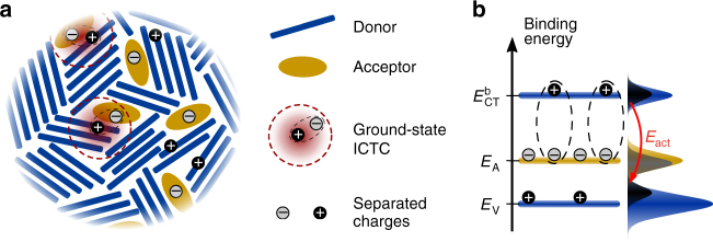
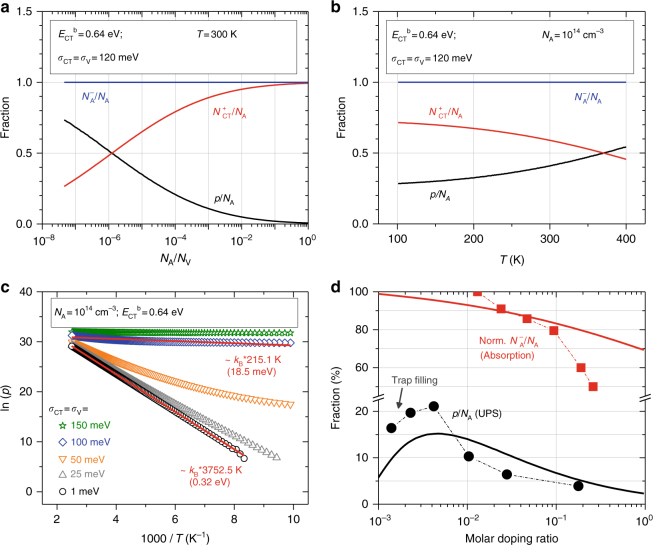
Fermi level control by doping is established since decades in inorganic semiconductors and has been successfully introduced in organic semiconductors. Despite its commercial success in the multi-billion OLED display business, molecular doping is little understood, with its elementary steps controversially discussed and mostly-empirical-materials design. Particularly puzzling is the efficient carrier release, despite a presumably large Coulomb barrier. Here we quantitatively investigate doping as a two-step process, involving single-electron transfer from donor to acceptor molecules and subsequent dissociation of the ground-state integer-charge transfer complex (ICTC). We show that carrier release by ICTC dissociation has an activation energy of only a few tens of meV, despite a Coulomb binding of several 100 meV. We resolve this discrepancy by taking energetic disorder into account. The overall doping process is explained by an extended semiconductor model in which occupation of ICTCs causes the classically known reserve regime at device-relevant doping concentrations.
几十年来,通过掺杂来控制费米能级在无机半导体中已得到确立,并已成功引入有机半导体。尽管其在价值数十亿美元的 OLED 显示器业务中取得了商业上的成功,但分子掺杂的理解却很少,其基本步骤存在争议,且大多是经验性的材料设计。尽管存在推测的大库仑势垒,但令人特别困惑的是有效载流子的释放。在这里,我们定量研究了掺杂作为一个两步过程,涉及从施主到受主分子的单电子转移,以及随后的基态整数电荷转移复合物(ICTC)的解离。我们表明,尽管库仑束缚为几个 100meV,但 ICTC 解离的载流子释放具有仅几十毫电子伏特的激活能。通过考虑能量无序,我们解决了这一差异。通过扩展半导体模型来解释整个掺杂过程,其中 ICTC 的占据导致了在与器件相关的掺杂浓度下经典的所谓储备区。