Faculty of Physics , University of Vienna , 1090 Vienna , Austria.
Centre for Materials Science and Nanotechnology , University of Oslo , NO-0349 Oslo , Norway.
Nano Lett. 2018 Aug 8;18(8):5319-5323. doi: 10.1021/acs.nanolett.8b02406. Epub 2018 Jul 3.
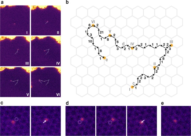
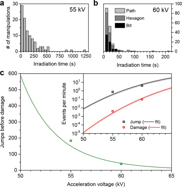
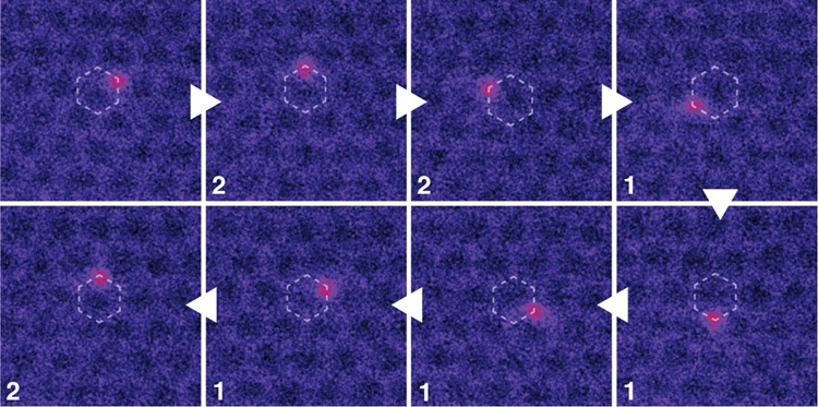
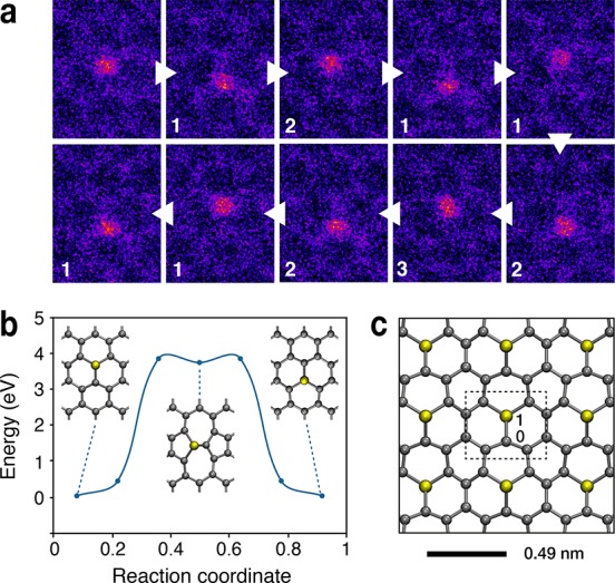
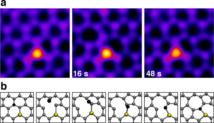
The direct manipulation of individual atoms in materials using scanning probe microscopy has been a seminal achievement of nanotechnology. Recent advances in imaging resolution and sample stability have made scanning transmission electron microscopy a promising alternative for single-atom manipulation of covalently bound materials. Pioneering experiments using an atomically focused electron beam have demonstrated the directed movement of silicon atoms over a handful of sites within the graphene lattice. Here, we achieve a much greater degree of control, allowing us to precisely move silicon impurities along an extended path, circulating a single hexagon, or back and forth between the two graphene sublattices. Even with manual operation, our manipulation rate is already comparable to the state-of-the-art in any atomically precise technique. We further explore the influence of electron energy on the manipulation rate, supported by improved theoretical modeling taking into account the vibrations of atoms near the impurities, and implement feedback to detect manipulation events in real time. In addition to atomic-level engineering of its structure and properties, graphene also provides an excellent platform for refining the accuracy of quantitative models and for the development of automated manipulation.
使用扫描探针显微镜直接操纵材料中的单个原子是纳米技术的一项重要成就。近年来,成像分辨率和样品稳定性的提高使得扫描透射电子显微镜成为共价键合材料单原子操纵的有前途的替代方法。使用原子聚焦电子束的开创性实验已经证明了硅原子在石墨烯晶格内少数几个位置上的定向运动。在这里,我们实现了更高程度的控制,使我们能够精确地沿着扩展路径移动硅杂质,循环一个单独的六边形,或者在两个石墨烯子晶格之间来回移动。即使采用手动操作,我们的操纵速度也已经与任何原子精度技术的最先进水平相当。我们进一步探讨了电子能量对操纵速度的影响,改进的理论模型考虑了杂质附近原子的振动,并且实现了反馈以实时检测操纵事件。除了对其结构和性质进行原子级工程设计外,石墨烯还为完善定量模型的准确性和开发自动化操纵提供了极好的平台。