• 文献检索
  • 文档翻译
  • 深度研究
  • 学术资讯
  • Suppr Zotero 插件Zotero 插件
  • 邀请有礼
  • 套餐&价格
  • 历史记录
应用&插件
Suppr Zotero 插件Zotero 插件浏览器插件Mac 客户端Windows 客户端微信小程序
定价
高级版会员购买积分包购买API积分包
服务
文献检索文档翻译深度研究API 文档MCP 服务
关于我们
关于 Suppr公司介绍联系我们用户协议隐私条款
关注我们

Suppr 超能文献

核心技术专利:CN118964589B侵权必究
粤ICP备2023148730 号-1Suppr @ 2026

文献检索

告别复杂PubMed语法,用中文像聊天一样搜索,搜遍4000万医学文献。AI智能推荐,让科研检索更轻松。

立即免费搜索

文件翻译

保留排版,准确专业,支持PDF/Word/PPT等文件格式,支持 12+语言互译。

免费翻译文档

深度研究

AI帮你快速写综述,25分钟生成高质量综述,智能提取关键信息,辅助科研写作。

立即免费体验

HfSe的缺陷与氧化的纳米尺度研究

Nanoscale Investigation of Defects and Oxidation of HfSe.

作者信息

Yao Qirong, Zhang Lijie, Bampoulis Pantelis, Zandvliet Harold J W

机构信息

Physics of Interfaces and Nanomaterials, MESA Institute for Nanotechnology, University of Twente, P.O. Box 217, 7500AE Enschede, The Netherlands.

School of Physics and Electronics, Hunan University, 410082 Changsha, China.

出版信息

J Phys Chem C Nanomater Interfaces. 2018 Nov 8;122(44):25498-25505. doi: 10.1021/acs.jpcc.8b08713. Epub 2018 Oct 18.

DOI:10.1021/acs.jpcc.8b08713
PMID:30450151
原文链接:https://pmc.ncbi.nlm.nih.gov/articles/PMC6231157/
Abstract

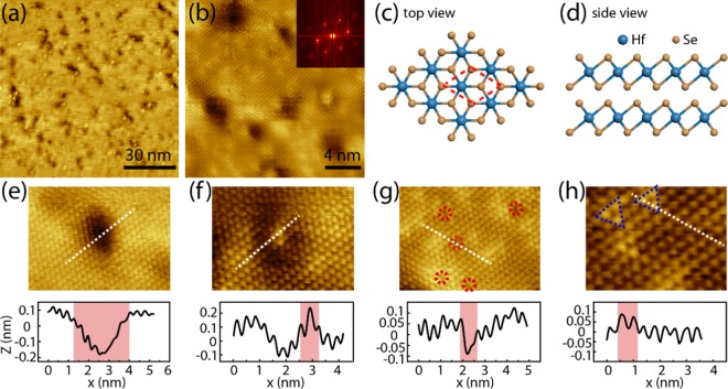
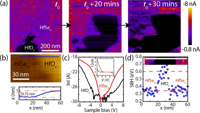
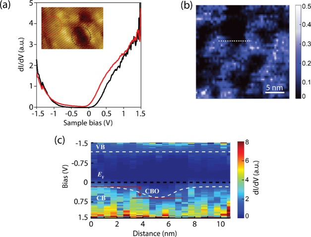
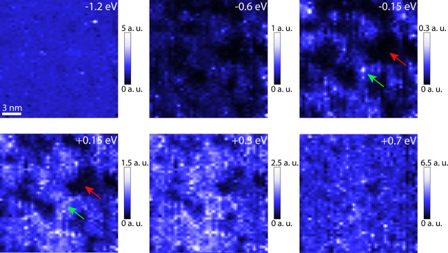
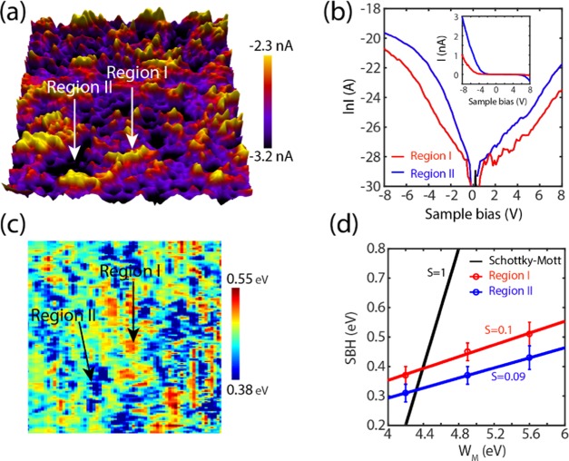
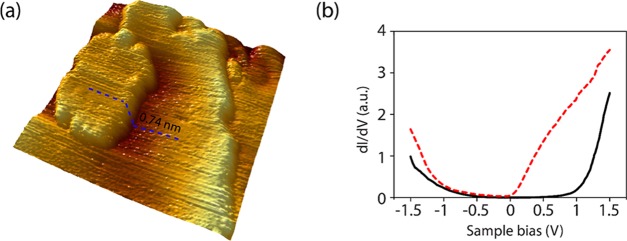
HfSe is a very good candidate for a transition metal dichalcogenide-based field-effect transistor owing to its moderate band gap of about 1 eV and its high-κ dielectric native oxide. Unfortunately, the experimentally determined charge carrier mobility is about 3 orders of magnitude lower than the theoretically predicted value. This strong deviation calls for a detailed investigation of the physical and electronic properties of HfSe. Here, we have studied the structure, density, and density of states of several types of defects that are abundant on the HfSe surface using scanning tunneling microscopy and spectroscopy. Compared to MoS and WSe, HfSe exhibits similar type of defects, albeit with a substantially higher density of 9 × 10 cm. The most abundant defect is a subsurface defect, which shows up as a dim feature in scanning tunneling microscopy images. These dim dark defects have a substantially larger band gap (1.25 eV) than the pristine surface (1 eV), suggesting a substitution of the Hf atom by another atom. The high density of defects on the HfSe surface leads to very low Schottky barrier heights. Conductive atomic force microscopy measurements reveal a very small dependence of the Schottky barrier height on the work function of the metals, suggesting a strong Fermi-level pinning. We attribute the observed Fermi-level pinning (pinning factor ∼0.1) to surface distortions and Se/Hf defects. In addition, we have also studied the HfSe surface after the exposure to air by scanning tunneling microscopy and conductive atomic force microscopy. Partly oxidized layers with band gaps of 2 eV and Schottky barrier heights of ∼0.6 eV were readily found on the surface. Our experiments reveal that HfSe is very air-sensitive, implying that capping or encapsulating of HfSe, in order to protect it against oxidation, is a necessity for technological applications.

摘要

由于HfSe具有约1 eV的适度带隙和高κ介电常数的原生氧化物,它是基于过渡金属二硫属化物的场效应晶体管的一个非常好的候选材料。不幸的是,实验测定的电荷载流子迁移率比理论预测值低约3个数量级。这种强烈的偏差需要对HfSe的物理和电子性质进行详细研究。在这里,我们使用扫描隧道显微镜和光谱学研究了HfSe表面大量存在的几种类型缺陷的结构、密度和态密度。与MoS和WSe相比,HfSe表现出类似类型的缺陷,尽管其密度高达9×10¹² cm⁻²。最丰富的缺陷是一种次表面缺陷,在扫描隧道显微镜图像中表现为暗淡特征。这些暗淡的暗缺陷具有比原始表面(1 eV)大得多的带隙(1.25 eV),表明Hf原子被另一个原子取代。HfSe表面的高密度缺陷导致非常低的肖特基势垒高度。导电原子力显微镜测量表明,肖特基势垒高度对金属功函数的依赖性非常小,表明存在强烈的费米能级钉扎。我们将观察到的费米能级钉扎(钉扎因子约为0.1)归因于表面畸变和Se/Hf缺陷。此外,我们还通过扫描隧道显微镜和导电原子力显微镜研究了暴露于空气中后的HfSe表面。在表面很容易发现带隙为2 eV且肖特基势垒高度约为0.6 eV的部分氧化层。我们的实验表明,HfSe对空气非常敏感,这意味着为了保护其免受氧化,对HfSe进行覆盖或封装对于技术应用来说是必要的。

https://cdn.ncbi.nlm.nih.gov/pmc/blobs/5d09/6231157/95ea389ac0e9/jp-2018-087137_0006.jpg
https://cdn.ncbi.nlm.nih.gov/pmc/blobs/5d09/6231157/ec5a6c2709bc/jp-2018-087137_0001.jpg
https://cdn.ncbi.nlm.nih.gov/pmc/blobs/5d09/6231157/4d0d8f4ba556/jp-2018-087137_0002.jpg
https://cdn.ncbi.nlm.nih.gov/pmc/blobs/5d09/6231157/453c63e37704/jp-2018-087137_0003.jpg
https://cdn.ncbi.nlm.nih.gov/pmc/blobs/5d09/6231157/9409a2793abe/jp-2018-087137_0004.jpg
https://cdn.ncbi.nlm.nih.gov/pmc/blobs/5d09/6231157/74df605cb679/jp-2018-087137_0005.jpg
https://cdn.ncbi.nlm.nih.gov/pmc/blobs/5d09/6231157/95ea389ac0e9/jp-2018-087137_0006.jpg

相似文献

1
Nanoscale Investigation of Defects and Oxidation of HfSe.HfSe的缺陷与氧化的纳米尺度研究
J Phys Chem C Nanomater Interfaces. 2018 Nov 8;122(44):25498-25505. doi: 10.1021/acs.jpcc.8b08713. Epub 2018 Oct 18.
2
Defect Dominated Charge Transport and Fermi Level Pinning in MoS/Metal Contacts.MoS/金属接触中的缺陷主导电荷输运和费米能级钉扎。
ACS Appl Mater Interfaces. 2017 Jun 7;9(22):19278-19286. doi: 10.1021/acsami.7b02739. Epub 2017 May 24.
3
Graphene contacts to a HfSe/SnS heterostructure.石墨烯与 HfSe/SnS 异质结构接触。
J Chem Phys. 2017 Feb 14;146(6):064701. doi: 10.1063/1.4975178.
4
Ambipolar MoS Transistors by Nanoscale Tailoring of Schottky Barrier Using Oxygen Plasma Functionalization.使用氧等离子体功能化纳米尺度调控肖特基势垒实现双极性 MoS 晶体管
ACS Appl Mater Interfaces. 2017 Jul 12;9(27):23164-23174. doi: 10.1021/acsami.7b04919. Epub 2017 Jun 26.
5
Strain-induced effects on the optoelectronic properties of ZrSe/HfSe heterostructures.应变对ZrSe/HfSe异质结构光电特性的影响。
J Mol Model. 2023 Dec 11;30(1):3. doi: 10.1007/s00894-023-05793-0.
6
Strong Fermi-Level Pinning in GeS-Metal Nanocontacts.GeS-金属纳米接触中的强费米能级钉扎
J Phys Chem C Nanomater Interfaces. 2022 Jul 14;126(27):11400-11406. doi: 10.1021/acs.jpcc.2c02827. Epub 2022 Jun 29.
7
High-κ Dielectric (HfO)/2D Semiconductor (HfSe) Gate Stack for Low-Power Steep-Switching Computing Devices.用于低功耗陡开关计算设备的高κ电介质(HfO)/二维半导体(HfSe)栅极堆叠
Adv Mater. 2024 Jun;36(26):e2312747. doi: 10.1002/adma.202312747. Epub 2024 Apr 8.
8
Carrier Polarity Control in α-MoTe2 Schottky Junctions Based on Weak Fermi-Level Pinning.基于弱费米能级钉扎的α-MoTe2 肖特基结中的载流子极性控制。
ACS Appl Mater Interfaces. 2016 Jun 15;8(23):14732-9. doi: 10.1021/acsami.6b02036. Epub 2016 Jun 2.
9
Band Structure Engineering of Layered WSe One-Step Chemical Functionalization.层状WSe的能带结构工程:一步化学功能化
ACS Nano. 2019 Jul 23;13(7):7545-7555. doi: 10.1021/acsnano.8b09351. Epub 2019 Jul 1.
10
Schottky Barrier Height Modulation Using Interface Characteristics of MoS Interlayer for Contact Structure.利用 MoS 层间的界面特性调制肖特基势垒高度用于接触结构。
ACS Appl Mater Interfaces. 2019 Feb 13;11(6):6230-6237. doi: 10.1021/acsami.8b18860. Epub 2019 Feb 1.

引用本文的文献

1
Advances and Applications of Oxidized van der Waals Transition Metal Dichalcogenides.氧化范德华过渡金属二硫属化物的进展与应用
Adv Sci (Weinh). 2024 Nov;11(43):e2407175. doi: 10.1002/advs.202407175. Epub 2024 Sep 23.
2
Plasma Processing and Treatment of 2D Transition Metal Dichalcogenides: Tuning Properties and Defect Engineering.二维过渡金属二硫属化物的等离子体处理与治疗:调控性能与缺陷工程
Chem Rev. 2023 Dec 27;123(24):13869-13951. doi: 10.1021/acs.chemrev.3c00147. Epub 2023 Dec 4.
3
Strong Fermi-Level Pinning in GeS-Metal Nanocontacts.

本文引用的文献

1
Superconductivity in Pristine 2H_{a}-MoS_{2} at Ultrahigh Pressure.超高压下原始2Hₐ-MoS₂中的超导性
Phys Rev Lett. 2018 Jan 19;120(3):037002. doi: 10.1103/PhysRevLett.120.037002.
2
Defect Structure of Localized Excitons in a WSe_{2} Monolayer.二硒化钨单层中局域激子的缺陷结构
Phys Rev Lett. 2017 Jul 28;119(4):046101. doi: 10.1103/PhysRevLett.119.046101. Epub 2017 Jul 25.
3
van der Waals Layered Materials: Opportunities and Challenges.范德华层状材料:机遇与挑战。
GeS-金属纳米接触中的强费米能级钉扎
J Phys Chem C Nanomater Interfaces. 2022 Jul 14;126(27):11400-11406. doi: 10.1021/acs.jpcc.2c02827. Epub 2022 Jun 29.
4
Low-Power Memristive Logic Device Enabled by Controllable Oxidation of 2D HfSe for In-Memory Computing.用于内存计算的基于二维HfSe可控氧化的低功耗忆阻逻辑器件
Adv Sci (Weinh). 2021 Aug;8(15):e2005038. doi: 10.1002/advs.202005038. Epub 2021 May 29.
ACS Nano. 2017 Dec 26;11(12):11803-11830. doi: 10.1021/acsnano.7b07436. Epub 2017 Dec 13.
4
Structure Re-determination and Superconductivity Observation of Bulk 1T MoS.块状 1T-MoS2 的结构重新确定和超导观察
Angew Chem Int Ed Engl. 2018 Jan 26;57(5):1232-1235. doi: 10.1002/anie.201710512. Epub 2018 Jan 2.
5
Defect passivation of transition metal dichalcogenides via a charge transfer van der Waals interface.通过电荷转移范德华界面实现过渡金属二硫属化物的缺陷钝化
Sci Adv. 2017 Oct 20;3(10):e1701661. doi: 10.1126/sciadv.1701661. eCollection 2017 Oct.
6
HfSe and ZrSe: Two-dimensional semiconductors with native high-κ oxides.HfSe和ZrSe:具有天然高κ氧化物的二维半导体。
Sci Adv. 2017 Aug 11;3(8):e1700481. doi: 10.1126/sciadv.1700481. eCollection 2017 Aug.
7
Defect Dominated Charge Transport and Fermi Level Pinning in MoS/Metal Contacts.MoS/金属接触中的缺陷主导电荷输运和费米能级钉扎。
ACS Appl Mater Interfaces. 2017 Jun 7;9(22):19278-19286. doi: 10.1021/acsami.7b02739. Epub 2017 May 24.
8
Fermi Level Pinning at Electrical Metal Contacts of Monolayer Molybdenum Dichalcogenides.单层二硫化钼的金属电接触中的费米能级钉扎。
ACS Nano. 2017 Feb 28;11(2):1588-1596. doi: 10.1021/acsnano.6b07159. Epub 2017 Jan 23.
9
Tunable electrical properties of multilayer HfSe field effect transistors by oxygen plasma treatment.通过氧等离子体处理调控多层 HfSe 场效应晶体管的电学性能。
Nanoscale. 2017 Jan 26;9(4):1645-1652. doi: 10.1039/c6nr08467b.
10
Surface Analysis of WSe Crystals: Spatial and Electronic Variability.WSe 晶体的表面分析:空间和电子变异性。
ACS Appl Mater Interfaces. 2016 Oct 5;8(39):26400-26406. doi: 10.1021/acsami.6b08847. Epub 2016 Sep 15.