Brillson Leonard, Cox Jonathan, Gao Hantian, Foster Geoffrey, Ruane William, Jarjour Alexander, Allen Martin, Look David, von Wenckstern Holger, Grundmann Marius
Department of Physics and Department of Electrical & Computer Engineering, The Ohio State University, Columbus, OH 43210, USA.
Department of Physics, The Ohio State University, Columbus, OH 43210, USA.
Materials (Basel). 2019 Jul 12;12(14):2242. doi: 10.3390/ma12142242.
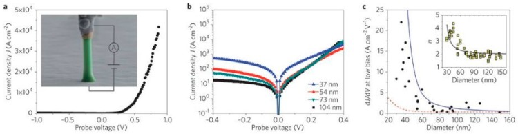
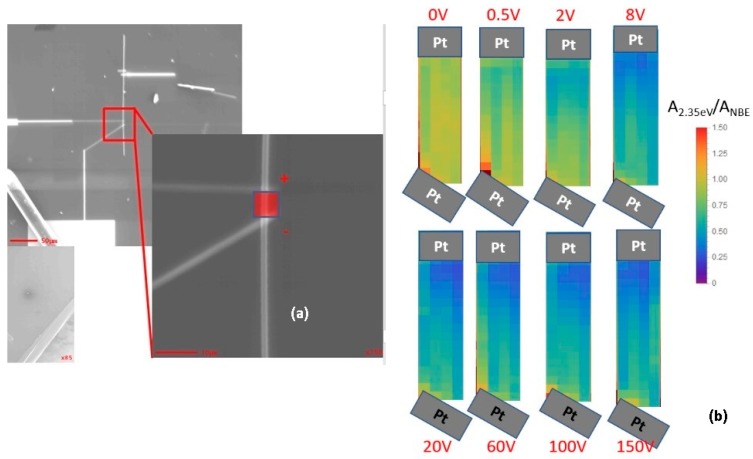
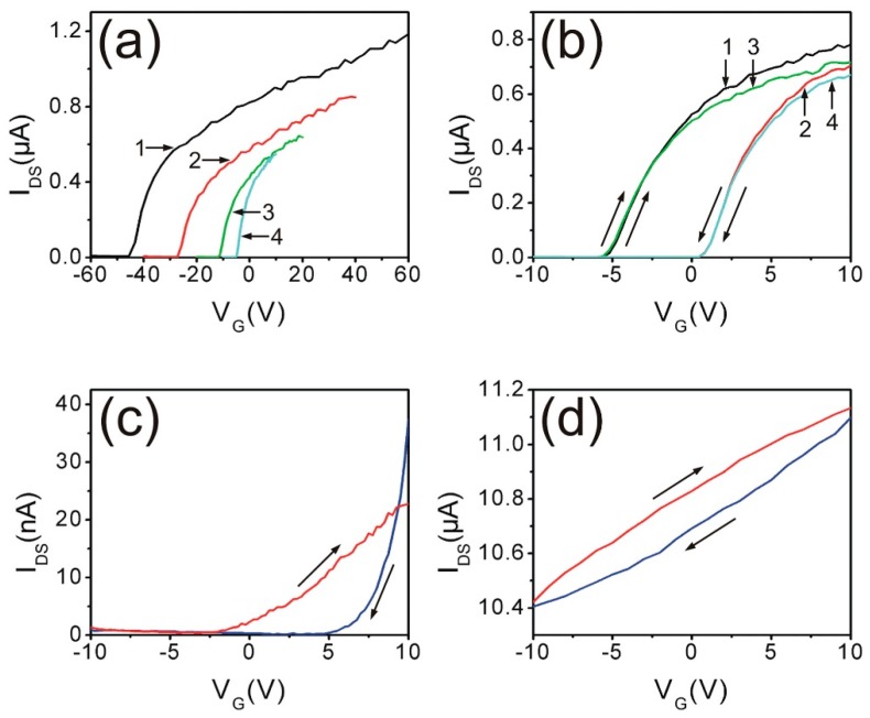
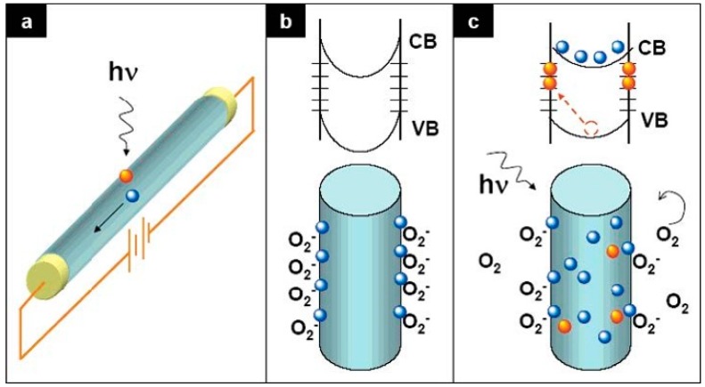
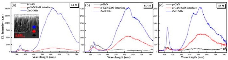
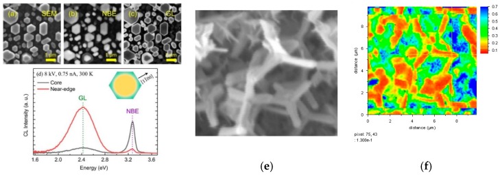
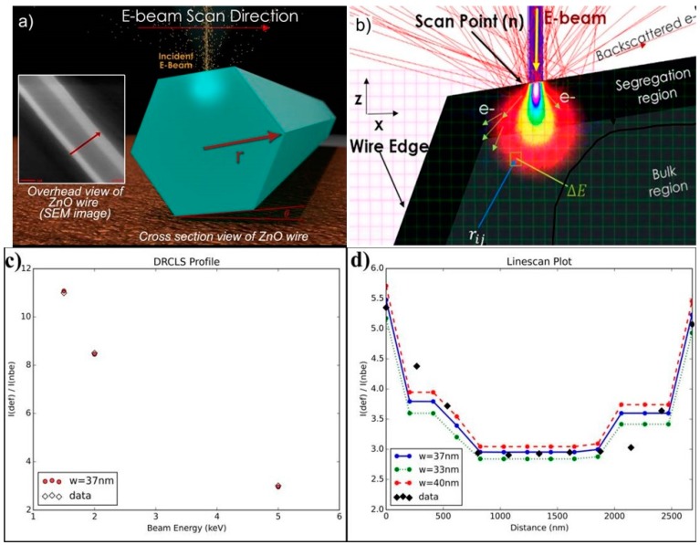
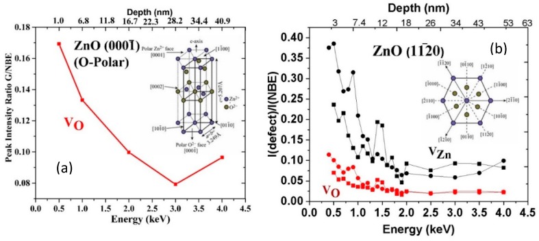
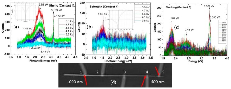
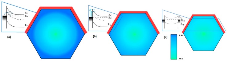
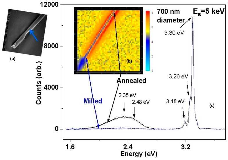
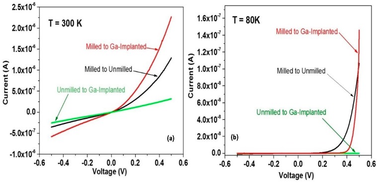
This review presents recent research advances in measuring native point defects in ZnO nanostructures, establishing how these defects affect nanoscale electronic properties, and developing new techniques to manipulate these defects to control nano- and micro- wire electronic properties. From spatially-resolved cathodoluminescence spectroscopy, we now know that electrically-active native point defects are present inside, as well as at the surfaces of, ZnO and other semiconductor nanostructures. These defects within nanowires and at their metal interfaces can dominate electrical contact properties, yet they are sensitive to manipulation by chemical interactions, energy beams, as well as applied electrical fields. Non-uniform defect distributions are common among semiconductors, and their effects are magnified in semiconductor nanostructures so that their electronic effects are significant. The ability to measure native point defects directly on a nanoscale and manipulate their spatial distributions by multiple techniques presents exciting possibilities for future ZnO nanoscale electronics.
本综述介绍了在测量ZnO纳米结构中的本征点缺陷、确定这些缺陷如何影响纳米级电子特性以及开发操纵这些缺陷以控制纳米线和微米线电子特性的新技术方面的最新研究进展。通过空间分辨阴极发光光谱法,我们现在知道电活性本征点缺陷存在于ZnO和其他半导体纳米结构的内部以及表面。纳米线内部及其金属界面处的这些缺陷可以主导电接触特性,但它们对化学相互作用、能量束以及外加电场的操纵很敏感。半导体中不均匀的缺陷分布很常见,并且它们的影响在半导体纳米结构中会被放大,因此它们的电子效应很显著。能够在纳米尺度上直接测量本征点缺陷并通过多种技术操纵其空间分布,为未来的ZnO纳米级电子学带来了令人兴奋的可能性。