Maximenko Sergey I, Moore Jim E, Affouda Chaffra A, Jenkins Phillip P
Naval Research Laboratory, Washington, DC, 20375, USA.
The George Washington University, Washington, DC, 20052, USA.
Sci Rep. 2019 Jul 26;9(1):10892. doi: 10.1038/s41598-019-47371-6.
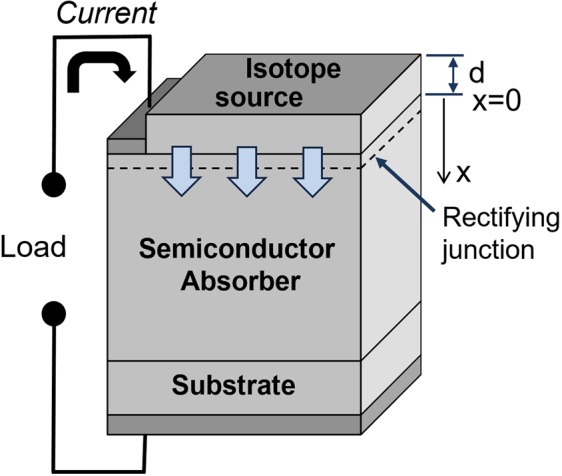
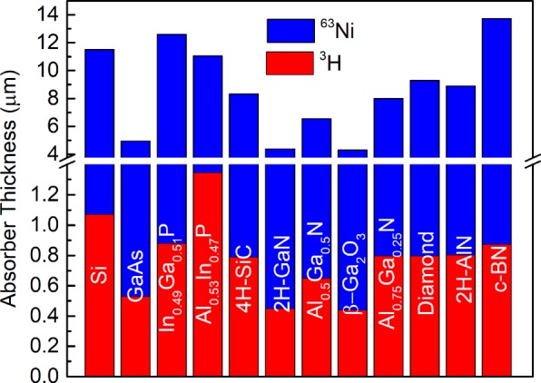
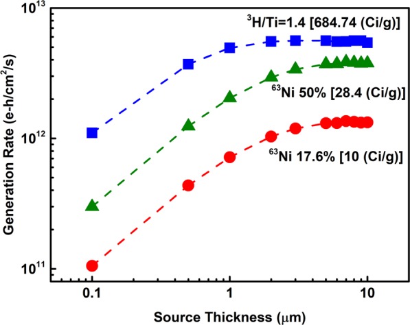
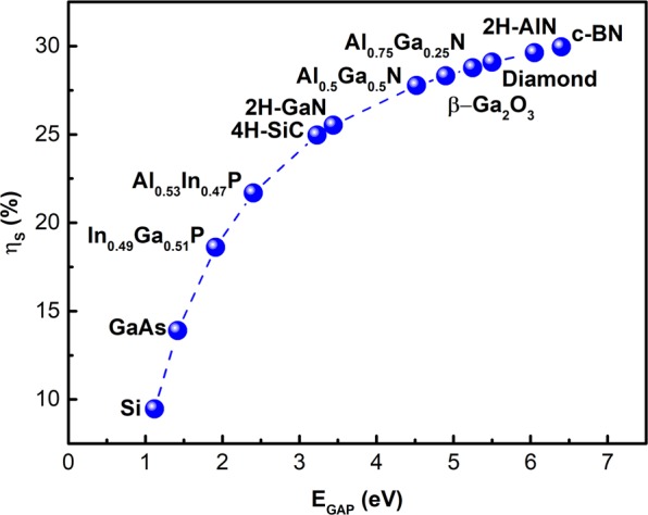
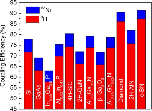
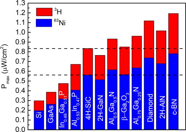
Betavoltaic power sources based on the conversion of radioisotope energy to electrical power are considered an appealing option for remote applications due to extended period of operation and high energy densities. However, to be competitive with other power sources, their efficiency must be increased. This can be done through optimization of the beta source and selection of the semiconductor absorber. This paper evaluates available on the market and developing wideband gap semiconductors as prospective absorbers with H and Ni sources. Simulation results indicate that among wide band gap materials 4H-SiC and diamond are two optimal semiconductors due to the combination of good coupling efficiencies with isotope sources and good electronic transport properties. Additionally, having good coupling efficiency, an ultra-wide bandgap, and the capability for both n- and p-type doping, c-BN is a promising material for betavoltaic applications.
基于将放射性同位素能量转换为电能的β伏特电源,因其运行时间长和能量密度高,被认为是远程应用的一个有吸引力的选择。然而,要与其他电源竞争,必须提高其效率。这可以通过优化β源和选择半导体吸收体来实现。本文评估了市场上现有的以及正在开发的宽带隙半导体作为与H和Ni源结合的潜在吸收体。模拟结果表明,在宽带隙材料中,4H-SiC和金刚石是两种最佳半导体,因为它们与同位素源具有良好的耦合效率,且电子传输性能良好。此外,立方氮化硼具有良好的耦合效率、超宽带隙以及n型和p型掺杂能力,是β伏特应用中一种很有前景的材料。