Kwon Soyeong, Kwon Min Hee, Song Jungeun, Kim Eunah, Kim Youngji, Kim Bo Ra, Hyun Jerome K, Lee Sang Wook, Kim Dong-Wook
Department of Physics, Ewha Womans University, Seoul, 03760, Korea.
Department of Chemistry and Nano Science, Ewha Womans University, Seoul, 03760, Korea.
Sci Rep. 2019 Oct 8;9(1):14434. doi: 10.1038/s41598-019-50950-2.
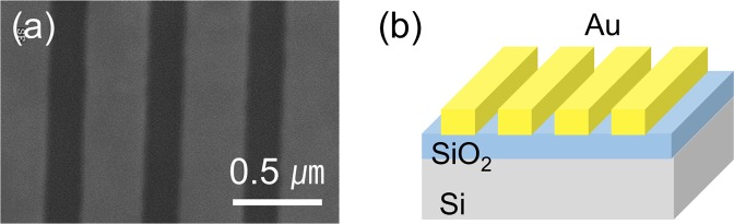
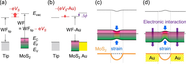
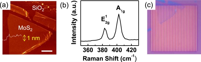
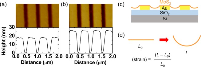
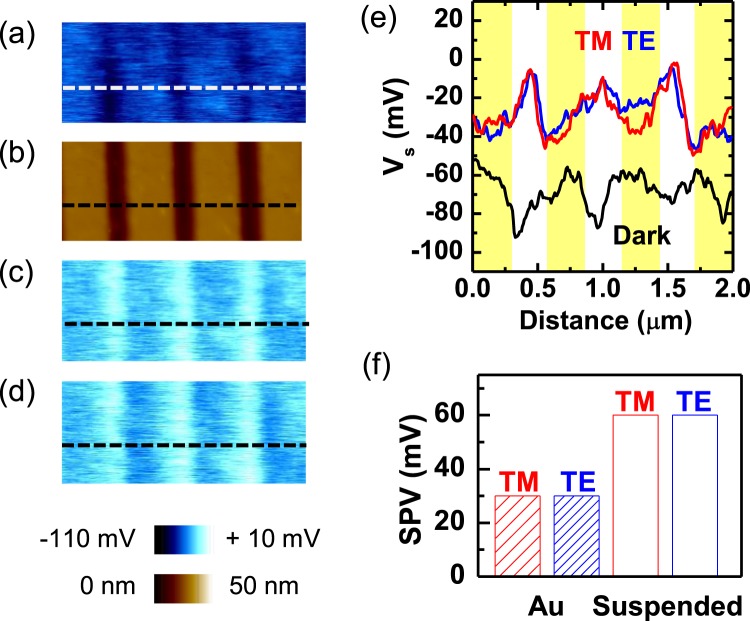
In this work, the surface potential (V) of exfoliated MoS monolayers on Au nanostripe arrays with period of 500 nm was investigated using Kelvin probe force microscopy. The surface morphology showed that the suspended MoS region between neighboring Au stripes underwent tensile-strain. In the dark, the V of the MoS region on the Au stripe (V-Au) was larger than that of the suspended MoS region (V-S). However, under green light illumination, V-Au became smaller than V-S. To explain the V modification, band diagrams have been constructed taking into consideration not only the local strain but also the electronic interaction at the MoS/Au interface. The results of this work provide a basis for understanding the electrical properties of MoS-metal contacts and improving the performance of MoS-based optoelectronic devices.
在这项工作中,使用开尔文探针力显微镜研究了周期为500纳米的金纳米条纹阵列上剥离的二硫化钼单层的表面电势(V)。表面形态表明,相邻金条纹之间的悬浮二硫化钼区域受到拉伸应变。在黑暗中,金条纹上二硫化钼区域的V(V-Au)大于悬浮二硫化钼区域的V(V-S)。然而,在绿光照射下,V-Au变得小于V-S。为了解释V的变化,构建了能带图,不仅考虑了局部应变,还考虑了二硫化钼/金界面处的电子相互作用。这项工作的结果为理解二硫化钼-金属接触的电学性质和提高基于二硫化钼的光电器件的性能提供了基础。