Engineering Research Center for Navigation Technology, Department of Precision Instrument, Tsinghua University, Beijing 100084, China.
College of Information Science and Engineering, Shandong Agricultural University, Tai'an 271018, China.
Sensors (Basel). 2020 Jan 14;20(2):462. doi: 10.3390/s20020462.
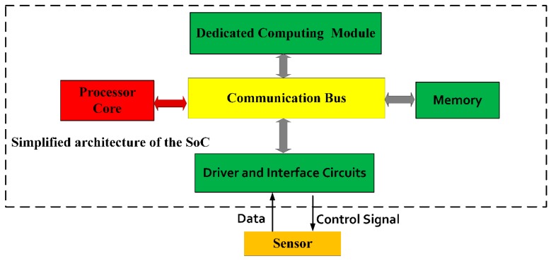
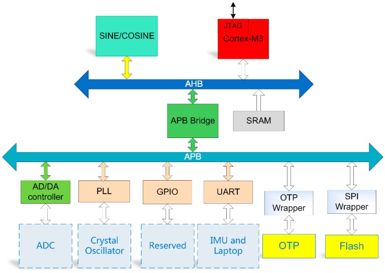
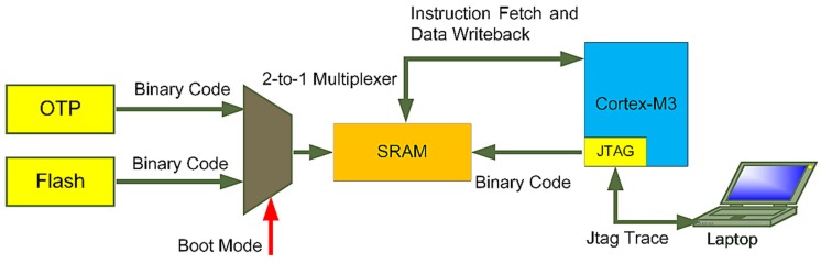
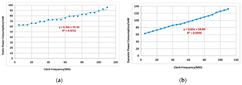
For signal processing of a Micro-Electro-Mechanical System (MEMS) Inertial Measurement Unit (IMU), a digital-analog hybrid system-on-chip (SoC) with small area and low power consumption was designed and implemented in this paper. To increase the flexibility of the processing circuit, the designed SoC integrates a low-power processor and supports three startup or debugging modes for different application scenarios. An application-specific computing module and communication interface are designed in the circuit to meet the requirements of IMU signal processing. The configurable clock allows users to dynamically balance computing speed and power consumption in their applications. The chip was taped out under SMIC 180 nm CMOS technology and tested for performance. The results show that the chip's maximum running frequency is 105 MHz. The total area is 33.94 mm2. The dynamic and static power consumption are 0.65 mW/MHz and 0.30 mW/MHz, respectively. When the system clock is 25 MHz, the dynamic and static power consumption of the chip is 76 mW and 66 mW, and the dynamic and static power consumption of the FPGA level are 634 mW and 520 mW. The results verify the superiority of the application specific integrated circuit (ASIC) solution in terms of integration and low power consumption.
针对微机电系统(MEMS)惯性测量单元(IMU)的信号处理,本文设计并实现了一款面积小、功耗低的数模混合系统级芯片(SoC)。为了提高处理电路的灵活性,所设计的 SoC 集成了低功耗处理器,并支持三种启动或调试模式,以满足不同应用场景的需求。在电路中设计了专用计算模块和通信接口,以满足 IMU 信号处理的要求。可配置的时钟允许用户在应用中动态平衡计算速度和功耗。该芯片采用 SMIC 180nm CMOS 工艺流片,并进行了性能测试。结果表明,该芯片的最高运行频率为 105MHz,总面积为 33.94mm2,动态和静态功耗分别为 0.65mW/MHz 和 0.30mW/MHz。当系统时钟为 25MHz 时,芯片的动态和静态功耗分别为 76mW 和 66mW,FPGA 级的动态和静态功耗分别为 634mW 和 520mW。结果验证了 ASIC 解决方案在集成度和低功耗方面的优势。