Jevtics Dimitars, McPhillimy John, Guilhabert Benoit, Alanis Juan A, Tan Hark Hoe, Jagadish Chennupati, Dawson Martin D, Hurtado Antonio, Parkinson Patrick, Strain Michael J
Institute of Photonics, SUPA Department of Physics, University of Strathclyde, Glasgow G1 1XQ, United Kingdom.
Department of Physics and Astronomy and Photon Science Institute, The University of Manchester, Manchester M13 9PL, United Kingdom.
Nano Lett. 2020 Mar 11;20(3):1862-1868. doi: 10.1021/acs.nanolett.9b05078. Epub 2020 Feb 14.
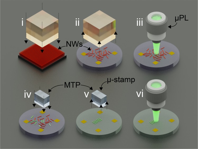
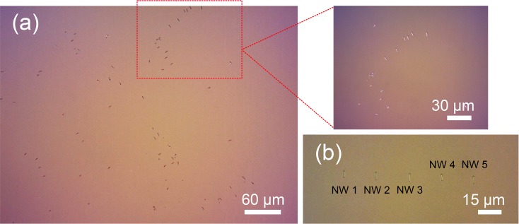
Semiconductor nanowire (NW) lasers are a promising technology for the realization of coherent optical sources with ultrasmall footprint. To fully realize their potential in on-chip photonic systems, scalable methods are required for dealing with large populations of inhomogeneous devices that are typically randomly distributed on host substrates. In this work two complementary, high-throughput techniques are combined: the characterization of nanowire laser populations using automated optical microscopy, and a high-accuracy transfer-printing process with automatic device spatial registration and transfer. Here, a population of NW lasers is characterized, binned by threshold energy density, and subsequently printed in arrays onto a secondary substrate. Statistical analysis of the transferred and control devices shows that the transfer process does not incur measurable laser damage, and the threshold binning can be maintained. Analysis on the threshold and mode spectra of the device populations proves the potential for using NW lasers for integrated systems fabrication.
半导体纳米线(NW)激光器是实现具有超小尺寸的相干光源的一项很有前景的技术。为了在片上光子系统中充分发挥其潜力,需要可扩展的方法来处理大量通常随机分布在宿主衬底上的不均匀器件。在这项工作中,两种互补的高通量技术被结合起来:使用自动光学显微镜对纳米线激光器群体进行表征,以及具有自动器件空间配准和转移功能的高精度转移印刷工艺。在这里,对一组NW激光器进行表征,按阈值能量密度进行分类,随后将其阵列印刷到第二个衬底上。对转移器件和对照器件的统计分析表明,转移过程不会造成可测量的激光损伤,并且可以维持阈值分类。对器件群体的阈值和模式光谱进行分析证明了使用NW激光器制造集成系统的潜力。