• 文献检索
  • 文档翻译
  • 深度研究
  • 学术资讯
  • Suppr Zotero 插件Zotero 插件
  • 邀请有礼
  • 套餐&价格
  • 历史记录
应用&插件
Suppr Zotero 插件Zotero 插件浏览器插件Mac 客户端Windows 客户端微信小程序
定价
高级版会员购买积分包购买API积分包
服务
文献检索文档翻译深度研究API 文档MCP 服务
关于我们
关于 Suppr公司介绍联系我们用户协议隐私条款
关注我们

Suppr 超能文献

核心技术专利:CN118964589B侵权必究
粤ICP备2023148730 号-1Suppr @ 2026

文献检索

告别复杂PubMed语法,用中文像聊天一样搜索,搜遍4000万医学文献。AI智能推荐,让科研检索更轻松。

立即免费搜索

文件翻译

保留排版,准确专业,支持PDF/Word/PPT等文件格式,支持 12+语言互译。

免费翻译文档

深度研究

AI帮你快速写综述,25分钟生成高质量综述,智能提取关键信息,辅助科研写作。

立即免费体验

采用超薄切片技术对层状材料的大面积平面内和平面外横截面进行稳健的样品制备。

Robust Sample Preparation of Large-Area In- and Out-of-Plane Cross Sections of Layered Materials with Ultramicrotomy.

作者信息

Cichocka Magdalena O, Bolhuis Maarten, van Heijst Sabrya E, Conesa-Boj Sonia

机构信息

Kavli Institute of Nanoscience, Delft University of Technology, 2628CJ Delft, The Netherlands.

出版信息

ACS Appl Mater Interfaces. 2020 Apr 1;12(13):15867-15874. doi: 10.1021/acsami.9b22586. Epub 2020 Mar 17.

DOI:10.1021/acsami.9b22586
PMID:32155046
原文链接:https://pmc.ncbi.nlm.nih.gov/articles/PMC7118708/
Abstract

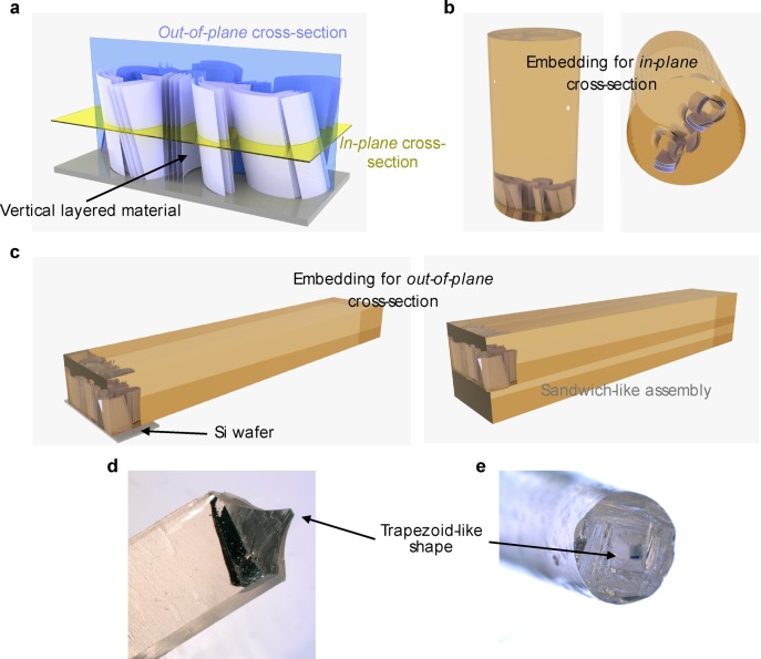
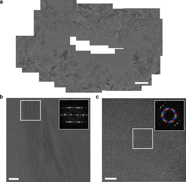
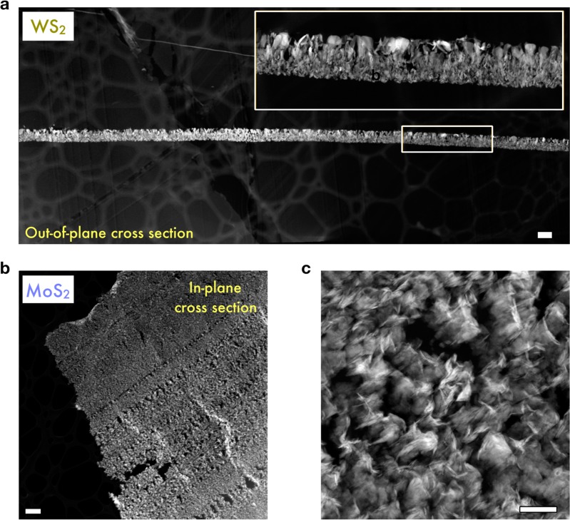
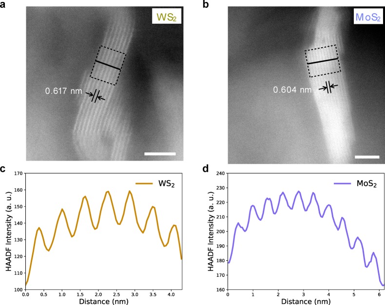
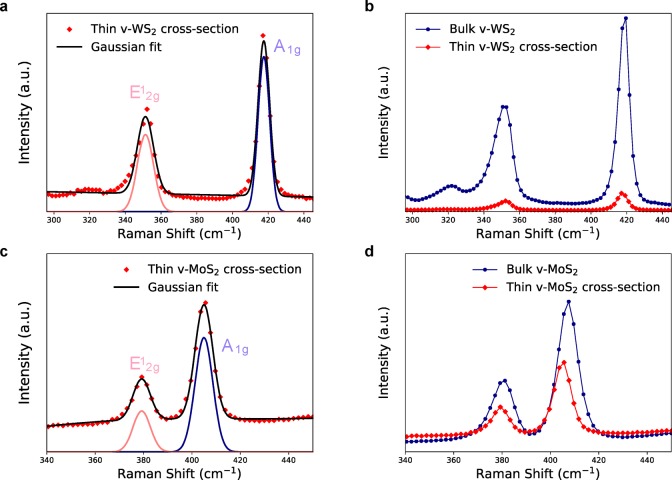
Layered materials (LMs) such as graphene or MoS have attracted a great deal of interest recently. These materials offer unique functionalities due to their structural anisotropy characterized by weak van der Waals bonds along the out-of-plane axis and covalent bonds in the in-plane direction. A central requirement to access the structural information on complex nanostructures built upon LMs is to control the relative orientation of each sample prior to their inspection, e.g., with transmission electron microscopy (TEM). However, developing sample preparation methods that result in large inspection areas and ensure full control over the sample orientation while avoiding damage during the transfer to the TEM grid is challenging. Here, we demonstrate the feasibility of deploying ultramicrotomy for the preparation of LM samples in TEM analyses. We show how ultramicrotomy leads to the reproducible large-scale production of both in-plane and out-of-plane cross sections, with bulk vertically oriented MoS and WS nanosheets as a proof of concept. The robustness of the prepared samples is subsequently verified by their characterization by means of both high-resolution TEM and Raman spectroscopy measurements. Our approach is fully general and should find applications for a wide range of materials as well as of techniques beyond TEM, thus paving the way to the systematic large-area mass-production of cross-sectional specimens for structural and compositional studies.

摘要

诸如石墨烯或二硫化钼之类的层状材料(LMs)近来引起了广泛关注。这些材料因其结构各向异性而具有独特功能,其特征是沿面外轴方向存在弱范德华键,而面内方向存在共价键。要获取基于层状材料构建的复杂纳米结构的结构信息,一个核心要求是在检查之前控制每个样品的相对取向,例如使用透射电子显微镜(TEM)。然而,开发能够产生大面积检查区域并确保对样品取向进行完全控制,同时避免在转移到TEM网格过程中造成损坏的样品制备方法具有挑战性。在此,我们展示了在TEM分析中采用超薄切片术制备层状材料样品的可行性。我们展示了超薄切片术如何实现可重复的大规模制备面内和面外横截面,以垂直取向的块状二硫化钼和二硫化钨纳米片作为概念验证。随后通过高分辨率TEM和拉曼光谱测量对制备的样品进行表征,验证了其稳定性。我们的方法具有通用性,应该能应用于广泛的材料以及TEM之外的技术,从而为用于结构和成分研究的横截面样品的系统大面积批量生产铺平道路。

https://cdn.ncbi.nlm.nih.gov/pmc/blobs/00be/7118708/43e45dc9414c/am9b22586_0005.jpg
https://cdn.ncbi.nlm.nih.gov/pmc/blobs/00be/7118708/04bcd01507d2/am9b22586_0001.jpg
https://cdn.ncbi.nlm.nih.gov/pmc/blobs/00be/7118708/733510a377c7/am9b22586_0002.jpg
https://cdn.ncbi.nlm.nih.gov/pmc/blobs/00be/7118708/2d330ff456ef/am9b22586_0003.jpg
https://cdn.ncbi.nlm.nih.gov/pmc/blobs/00be/7118708/ac4e5daf8dda/am9b22586_0004.jpg
https://cdn.ncbi.nlm.nih.gov/pmc/blobs/00be/7118708/43e45dc9414c/am9b22586_0005.jpg

相似文献

1
Robust Sample Preparation of Large-Area In- and Out-of-Plane Cross Sections of Layered Materials with Ultramicrotomy.采用超薄切片技术对层状材料的大面积平面内和平面外横截面进行稳健的样品制备。
ACS Appl Mater Interfaces. 2020 Apr 1;12(13):15867-15874. doi: 10.1021/acsami.9b22586. Epub 2020 Mar 17.
2
Cross-Plane Carrier Transport in Van der Waals Layered Materials.范德华层状材料中的跨平面载流子输运
Small. 2018 May;14(20):e1703808. doi: 10.1002/smll.201703808. Epub 2018 Apr 16.
3
Combined Focused Ion Beam-Ultramicrotomy Method for TEM Specimen Preparation of Porous Fine-Grained Materials.用于多孔细粒材料透射电子显微镜样品制备的聚焦离子束-超薄切片联合方法
Microsc Microanal. 2020 Feb;26(1):120-125. doi: 10.1017/S1431927619015186.
4
Comparative Sample Preparation Using Focused Ion Beam and Ultramicrotomy of Human Dental Enamel and Dentine for Multimicroscopic Imaging at Micro- and Nanoscale.使用聚焦离子束和超薄切片技术对人牙釉质和牙本质进行比较样本制备,用于微观和纳米尺度的多显微镜成像。
Materials (Basel). 2022 Apr 24;15(9):3084. doi: 10.3390/ma15093084.
5
Facilitating Uniform Large-Scale MoS, WS Monolayers, and Their Heterostructures through van der Waals Epitaxy.通过范德华外延法制备均匀的大规模二硫化钼、二硫化钨单层及其异质结构。
ACS Appl Mater Interfaces. 2022 Sep 21;14(37):42365-42373. doi: 10.1021/acsami.2c12174. Epub 2022 Sep 8.
6
Transition metal dichalcogenides and beyond: synthesis, properties, and applications of single- and few-layer nanosheets.过渡金属二卤化物及其以外的单层和少层纳米片的合成、性质和应用。
Acc Chem Res. 2015 Jan 20;48(1):56-64. doi: 10.1021/ar5002846. Epub 2014 Dec 9.
7
Band Alignment and Minigaps in Monolayer MoS2-Graphene van der Waals Heterostructures.单层 MoS2-石墨烯范德华异质结构中的能带排列和能隙
Nano Lett. 2016 Jul 13;16(7):4054-61. doi: 10.1021/acs.nanolett.6b00609. Epub 2016 Jun 16.
8
Nanotubes from chalcogenide misfit compounds: Sn-S and Nb-Pb-S.碲化物错位化合物的纳米管:Sn-S 和 Nb-Pb-S。
Acc Chem Res. 2014 Feb 18;47(2):406-16. doi: 10.1021/ar400138h. Epub 2013 Sep 17.
9
Large area growth of vertically aligned luminescent MoS nanosheets.大面积垂直排列发光 MoS 纳米片的生长。
Nanoscale. 2017 Jan 7;9(1):277-287. doi: 10.1039/c6nr07965b. Epub 2016 Dec 1.
10
Planning Implications Related to Sterilization-Sensitive Science Investigations Associated with Mars Sample Return (MSR).与火星样本返回(MSR)相关的对灭菌敏感的科学研究的规划意义。
Astrobiology. 2022 Jun;22(S1):S112-S164. doi: 10.1089/AST.2021.0113. Epub 2022 May 19.

引用本文的文献

1
Enhancement of Photocurrent Stability in Oxidation-Resistant WSeTe Nanosheets.提高抗氧化WSeTe纳米片中光电流的稳定性。
ACS Omega. 2025 Jun 13;10(24):26079-26089. doi: 10.1021/acsomega.5c02983. eCollection 2025 Jun 24.
2
Automatic tiling method for mosaic ceramic art images based on subpixel edge fitting localization and collaborative operation of multiple manipulators.基于亚像素边缘拟合定位与多机械手协同操作的马赛克陶瓷艺术图像自动拼接方法
Sci Rep. 2024 Oct 5;14(1):23215. doi: 10.1038/s41598-024-74567-2.

本文引用的文献

1
Tuning the orientation of few-layer MoS films using one-zone sulfurization.采用单区硫化法调控少层MoS薄膜的取向
RSC Adv. 2019 Sep 19;9(51):29645-29651. doi: 10.1039/c9ra06770a. eCollection 2019 Sep 18.
2
Vertically-oriented MoS nanosheets for nonlinear optical devices.用于非线性光学器件的垂直取向二硫化钼纳米片。
Nanoscale. 2020 May 21;12(19):10491-10497. doi: 10.1039/d0nr00755b. Epub 2020 May 7.
3
Metallic edge states in zig-zag vertically-oriented MoS nanowalls.之字形垂直取向的MoS纳米壁中的金属边缘态
Sci Rep. 2019 Oct 30;9(1):15602. doi: 10.1038/s41598-019-52119-3.
4
Phase Transformation Behavior of a Two-Dimensional Zeolite.二维沸石的相变行为
Angew Chem Int Ed Engl. 2019 Jul 22;58(30):10230-10235. doi: 10.1002/anie.201904825. Epub 2019 Jun 24.
5
WS Nanotubes, 2D Nanomeshes, and 2D In-Plane Films through One Single Chemical Vapor Deposition Route.通过单一化学气相沉积路线制备WS纳米管、二维纳米网和二维平面内薄膜。
ACS Nano. 2019 Apr 23;13(4):3896-3909. doi: 10.1021/acsnano.8b06515. Epub 2019 Apr 10.
6
Atomic electrostatic maps of 1D channels in 2D semiconductors using 4D scanning transmission electron microscopy.利用 4D 扫描透射电子显微镜观察二维半导体中 1D 通道的原子静电映射图。
Nat Commun. 2019 Mar 8;10(1):1127. doi: 10.1038/s41467-019-08904-9.
7
Understanding the exfoliation and dispersion of MoS nanosheets in pure water.理解 MoS 纳米片在纯水中的剥落和分散。
J Colloid Interface Sci. 2018 May 1;517:204-212. doi: 10.1016/j.jcis.2017.11.013. Epub 2017 Nov 6.
8
Growth of Wafer-Scale Standing Layers of WS for Self-Biased High-Speed UV-Visible-NIR Optoelectronic Devices.晶圆级 WS 体层生长用于自偏置高速紫外可见近红外光电设备。
ACS Appl Mater Interfaces. 2018 Jan 31;10(4):3964-3974. doi: 10.1021/acsami.7b16397. Epub 2018 Jan 16.
9
Atomic-Resolution Spectrum Imaging of Semiconductor Nanowires.半导体纳米线的原子分辨能谱成像。
Nano Lett. 2018 Mar 14;18(3):1557-1563. doi: 10.1021/acs.nanolett.7b03929. Epub 2017 Nov 13.
10
Strain-Dependent Edge Structures in MoS Layers.应变依赖的 MoS 层边缘结构。
Nano Lett. 2017 Nov 8;17(11):7021-7026. doi: 10.1021/acs.nanolett.7b03627. Epub 2017 Oct 26.