Dhawan Amit Raj, Belacel Cherif, Esparza-Villa Juan Uriel, Nasilowski Michel, Wang Zhiming, Schwob Catherine, Hugonin Jean-Paul, Coolen Laurent, Dubertret Benoît, Senellart Pascale, Maître Agnès
1Institute of Fundamental and Frontier Sciences, University of Electronic Science and Technology of China, Chengdu, 610054 People's Republic of China.
2Sorbonne Université, CNRS, Institut des Nanosciences de Paris, UMR 7588, 75005 Paris, France.
Light Sci Appl. 2020 Mar 4;9:33. doi: 10.1038/s41377-020-0269-0. eCollection 2020.
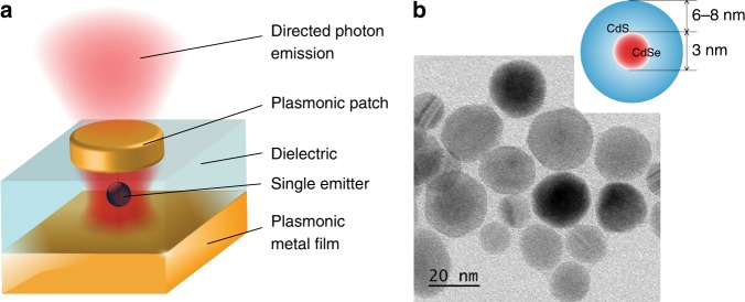
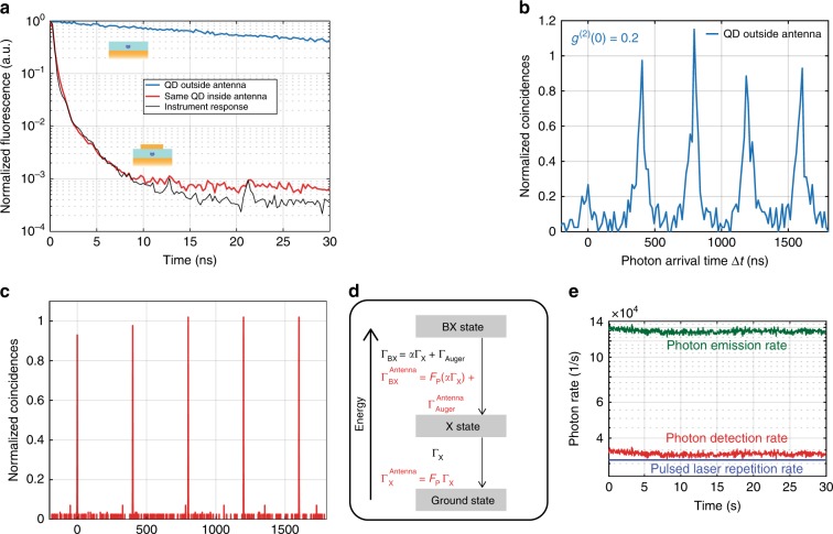
Coupling nano-emitters to plasmonic antennas is a key milestone for the development of nanoscale quantum light sources. One challenge, however, is the precise nanoscale positioning of the emitter in the structure. Here, we present a laser etching protocol that deterministically positions a single colloidal CdSe/CdS core/shell quantum dot emitter inside a subwavelength plasmonic patch antenna with three-dimensional nanoscale control. By exploiting the properties of metal-insulator-metal structures at the nanoscale, the fabricated single-emitter antenna exhibits a very high-Purcell factor (>72) and a brightness enhancement of a factor of 70. Due to the unprecedented quenching of Auger processes and the strong acceleration of the multiexciton emission, more than 4 photons per pulse can be emitted by a single quantum dot, thus increasing the device yield. Our technology can be applied to a wide range of photonic nanostructures and emitters, paving the way for scalable and reliable fabrication of ultra-compact light sources.
将纳米发射器与等离子体天线耦合是纳米级量子光源发展的一个关键里程碑。然而,一个挑战是发射器在结构中的精确纳米级定位。在此,我们提出一种激光蚀刻方案,该方案能在具有三维纳米级控制的亚波长等离子体贴片天线内确定性地定位单个胶体CdSe/CdS核壳量子点发射器。通过利用纳米尺度下金属 - 绝缘体 - 金属结构的特性,所制备的单发射器天线展现出非常高的珀塞尔因子(>72)以及70倍的亮度增强。由于俄歇过程前所未有的猝灭以及多激子发射的强烈加速,单个量子点每脉冲可发射超过4个光子,从而提高了器件产量。我们的技术可应用于广泛的光子纳米结构和发射器,为超紧凑型光源的可扩展且可靠的制造铺平了道路。