Han Tao, Liu Hongxia, Chen Shupeng, Chen Yanning, Wang Shulong, Li Zhandong
Key Laboratory for Wide-Band Gap Semiconductor Materials and Devices of Education, School of Microelectronics, Xidian University, Xi'an 710071, China.
State Grid Key Laboratory of Power Industrial Chip Design and Analysis Technology, Beijing Smart-Chip Microelectronics Technology Co., Ltd., Beijing 100192, China.
Micromachines (Basel). 2020 Dec 16;11(12):1114. doi: 10.3390/mi11121114.
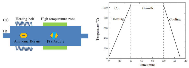
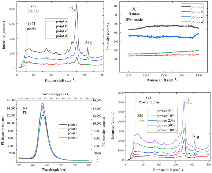
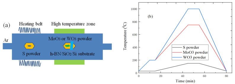
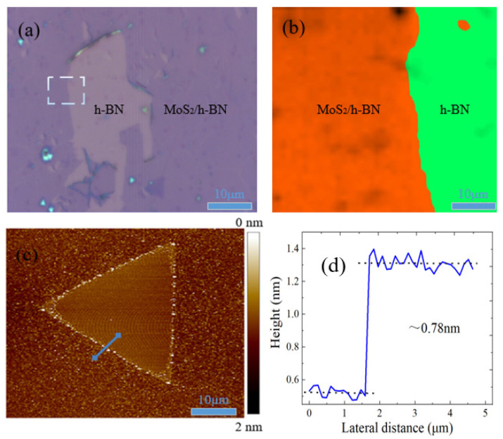
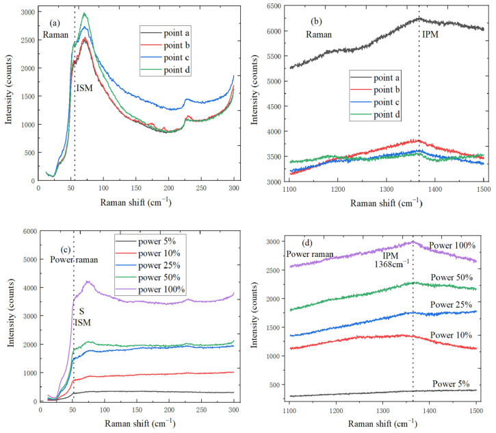
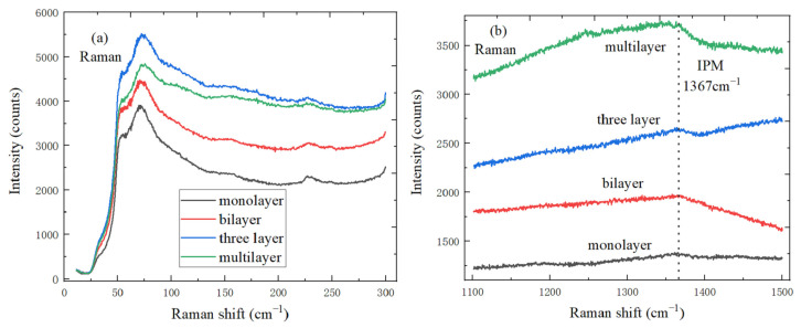
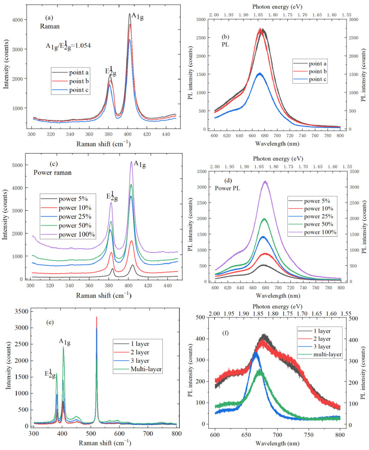
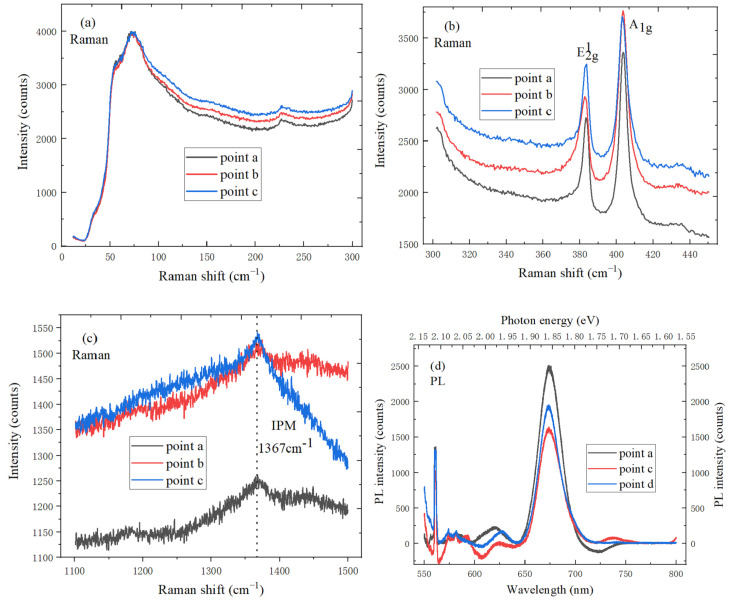
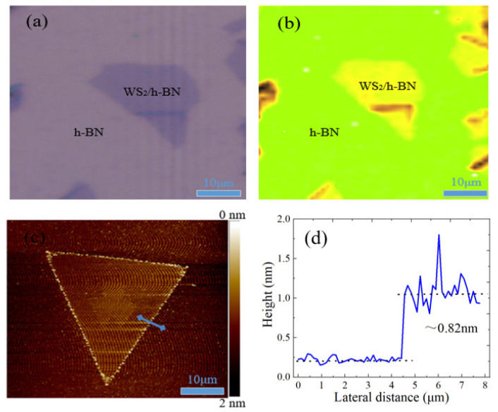
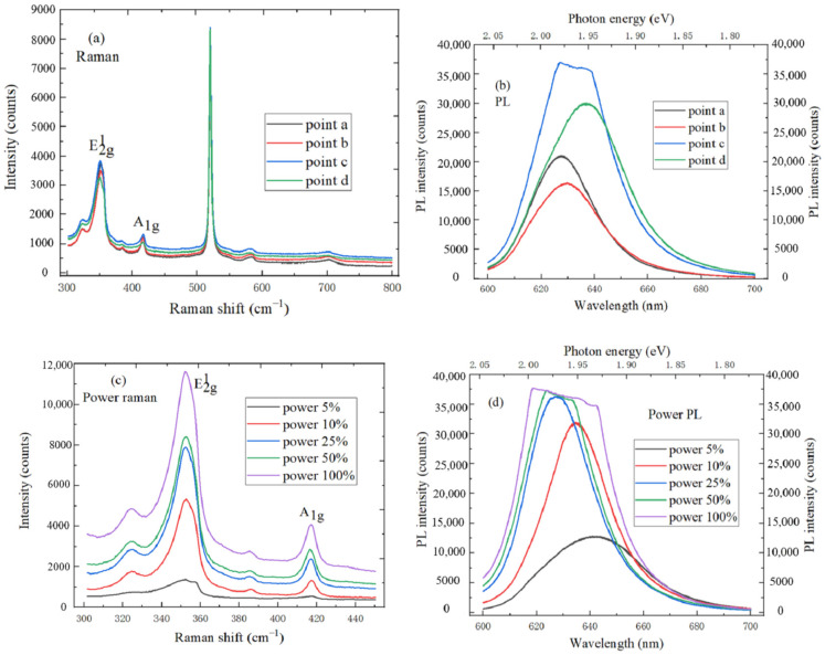
The general preparation method of large-area, continuous, uniform, and controllable vdW heterostructure materials is provided in this paper. To obtain the preparation of MoS/h-BN and WS/h-BN heterostructures, MoS and WS material are directly grown on the insulating h-BN substrate by atmospheric pressure chemical vapor deposition (APCVD) method, which does not require any intermediate transfer steps. The test characterization of MoS/h-BN and WS/h-BN vdW heterostructure materials can be accomplished by optical microscope, AFM, Raman and PL spectroscopy. The Raman peak signal of h-BN material is stronger when the h-BN film is thicker. Compared to the spectrum of MoS or WS material on SiO/Si substrate, the Raman and PL spectrum peak positions of MoS/h-BN heterostructure are blue-shifted, which is due to the presence of local strain, charged impurities and the vdW heterostructure interaction. Additionally, the PL spectrum of WS material shows the strong emission peak at 1.96 eV, while the full width half maximum (FWHM) is only 56 meV. The sharp emission peak indicates that WS/h-BN heterostructure material has the high crystallinity and clean interface. In addition, the peak position and shape of IPM mode characteristic peak are not obvious, which can be explained by the Van der Waals interaction of WS/h-BN heterostructure. From the above experimental results, the preparation method of heterostructure material is efficient and scalable, which can provide the important support for the subsequent application of TMDs/h-BN heterostructure in nanoelectronics and optoelectronics.
本文提供了大面积、连续、均匀且可控的范德华异质结构材料的一般制备方法。为了获得MoS/h-BN和WS/h-BN异质结构的制备,通过常压化学气相沉积(APCVD)方法将MoS和WS材料直接生长在绝缘的h-BN衬底上,该方法不需要任何中间转移步骤。MoS/h-BN和WS/h-BN范德华异质结构材料的测试表征可以通过光学显微镜、原子力显微镜、拉曼光谱和光致发光光谱来完成。当h-BN膜较厚时,h-BN材料的拉曼峰信号更强。与SiO/Si衬底上的MoS或WS材料的光谱相比,MoS/h-BN异质结构的拉曼光谱和光致发光光谱峰位发生蓝移,这是由于存在局部应变、带电杂质和范德华异质结构相互作用。此外,WS材料的光致发光光谱在1.96 eV处显示出强发射峰,而半高宽(FWHM)仅为56 meV。尖锐的发射峰表明WS/h-BN异质结构材料具有高结晶度和清洁界面。此外,IPM模式特征峰的峰位和形状不明显,这可以用WS/h-BN异质结构的范德华相互作用来解释。从上述实验结果来看,异质结构材料的制备方法高效且可扩展,可为TMDs/h-BN异质结构在纳米电子学和光电子学中的后续应用提供重要支持。