Sebbag Yoel, Talker Eliran, Naiman Alex, Barash Yefim, Levy Uriel
Department of Applied Physics, The Center for Nanoscience and Nanotechnology, The Hebrew University of Jerusalem, Jerusalem, 91904, Israel.
Light Sci Appl. 2021 Mar 11;10(1):54. doi: 10.1038/s41377-021-00499-5.
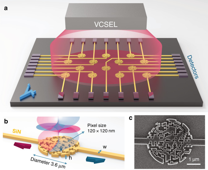
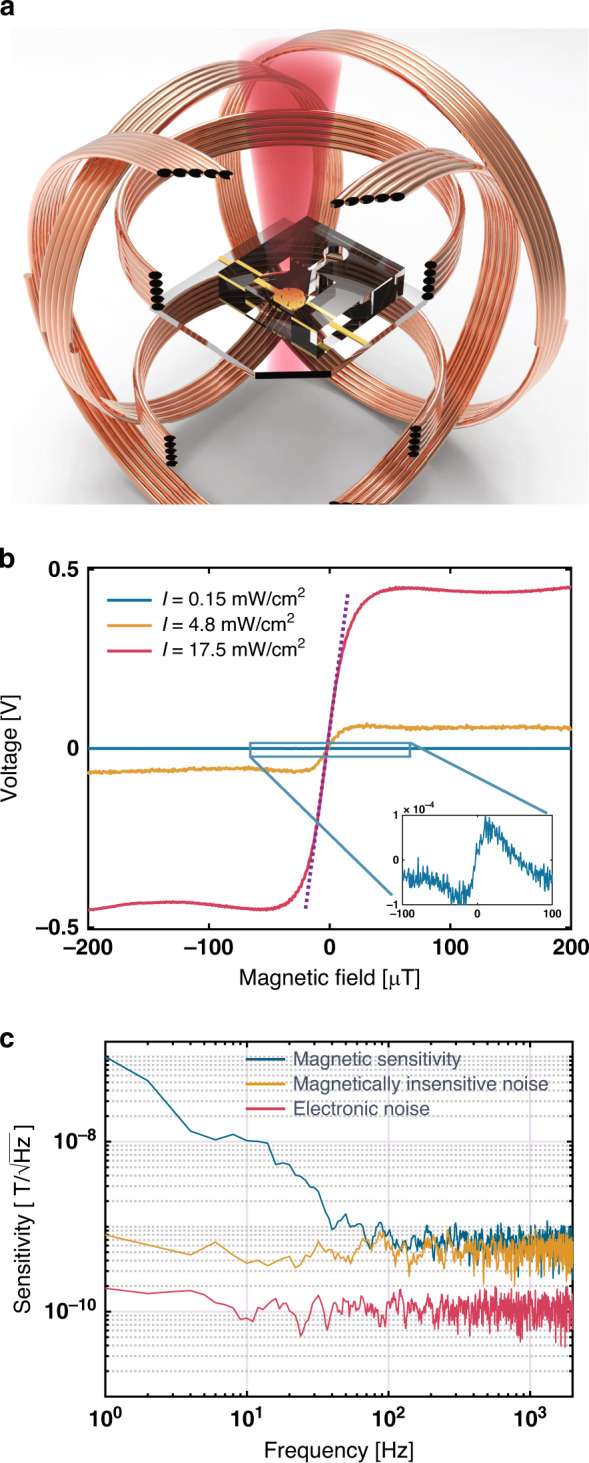
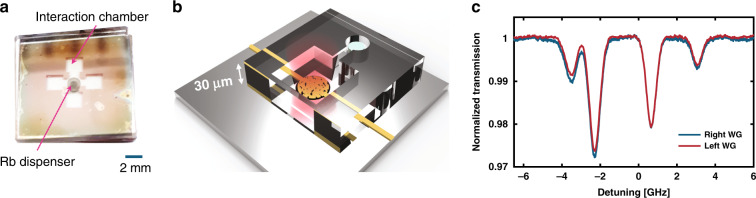
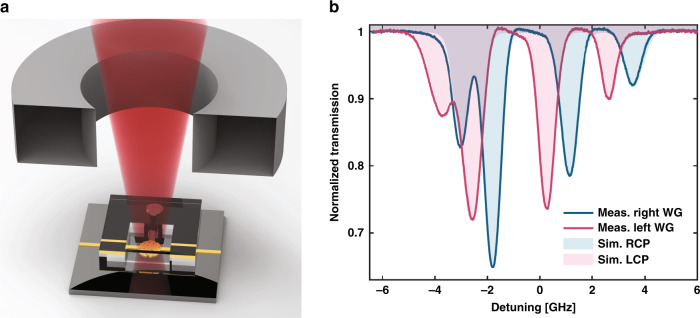
Recently, there has been growing interest in the miniaturization and integration of atomic-based quantum technologies. In addition to the obvious advantages brought by such integration in facilitating mass production, reducing the footprint, and reducing the cost, the flexibility offered by on-chip integration enables the development of new concepts and capabilities. In particular, recent advanced techniques based on computer-assisted optimization algorithms enable the development of newly engineered photonic structures with unconventional functionalities. Taking this concept further, we hereby demonstrate the design, fabrication, and experimental characterization of an integrated nanophotonic-atomic chip magnetometer based on alkali vapor with a micrometer-scale spatial resolution and a magnetic sensitivity of 700 pT/√Hz. The presented platform paves the way for future applications using integrated photonic-atomic chips, including high-spatial-resolution magnetometry, near-field vectorial imaging, magnetically induced switching, and optical isolation.
最近,人们对基于原子的量子技术的小型化和集成越来越感兴趣。除了这种集成在促进大规模生产、减小占地面积和降低成本方面带来的明显优势外,片上集成所提供的灵活性还能够开发新的概念和功能。特别是,基于计算机辅助优化算法的最新先进技术能够开发具有非常规功能的新型工程光子结构。进一步拓展这一概念,我们在此展示了一种基于碱金属蒸汽的集成纳米光子 - 原子芯片磁力计的设计、制造及实验表征,其具有微米级的空间分辨率和700 pT/√Hz的磁灵敏度。所展示的平台为未来使用集成光子 - 原子芯片的应用铺平了道路,包括高空间分辨率磁力测量、近场矢量成像、磁诱导开关和光学隔离。