Zhang Zengxing, Liu Guohua, Wang Kaiying
Department of microsystems, University of South-Eastern Norway, 3184 Horten, Norway.
Beijing Key Laboratory of Multiphase Flow and Heat Transfer for Low Grade Energy Utilization, North China Electric Power University, Beijing 102206, China.
Micromachines (Basel). 2021 Aug 25;12(9):1009. doi: 10.3390/mi12091009.
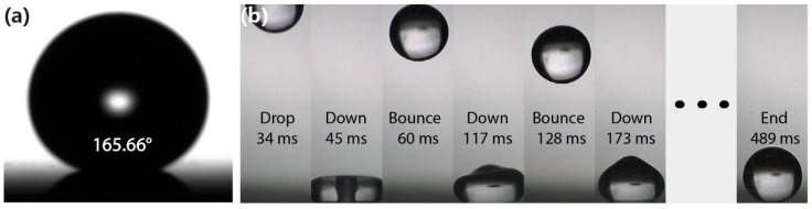
In this work, a modified Bosch etching process is developed to create silicon nanowires. Au nanoparticles (NPs) formed by magnetron sputtering film deposition and thermal annealing were employed as the hard mask to achieve controllable density and high aspect ratios. Such silicon nanowire exhibits the excellent anti-reflection ability of a reflectance value of below 2% within a broad light wave range between 220 and 1100 nm. In addition, Au NPs-induced surface plasmons significantly enhance the near-unity anti-reflection characteristics, achieving a reflectance below 3% within the wavelength range of 220 to 2600 nm. Furthermore, the nanowire array exhibits super-hydrophobic behavior with a contact angle over ~165.6° without enforcing any hydrophobic chemical treatment. Such behavior yields in water droplets bouncing off the surface many times. These properties render this silicon nanowire attractive for applications such as photothermal, photocatalysis, supercapacitor, and microfluidics.
在这项工作中,开发了一种改进的博世蚀刻工艺来制备硅纳米线。通过磁控溅射薄膜沉积和热退火形成的金纳米颗粒(NPs)被用作硬掩膜,以实现可控的密度和高纵横比。这种硅纳米线在220至1100nm的宽光波范围内表现出优异的抗反射能力,反射率值低于2%。此外,金纳米颗粒诱导的表面等离子体显著增强了近乎完全的抗反射特性,在220至2600nm的波长范围内实现了低于3%的反射率。此外,纳米线阵列表现出超疏水行为,接触角超过约165.6°,无需进行任何疏水化学处理。这种行为使得水滴能够多次从表面弹起。这些特性使得这种硅纳米线在光热、光催化、超级电容器和微流体等应用中具有吸引力。