Romanov Roman I, Kozodaev Maxim G, Chernikova Anna G, Zabrosaev Ivan V, Chouprik Anastasia A, Zarubin Sergey S, Novikov Sergey M, Volkov Valentyn S, Markeev Andrey M
Moscow Institute of Physics and Technology (National Research University), Institutskii per. 9, 141701 Dolgoprudny, Moscow Region, Russia.
ACS Omega. 2021 Dec 9;6(50):34429-34437. doi: 10.1021/acsomega.1c04532. eCollection 2021 Dec 21.
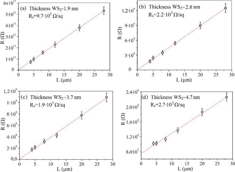
Ultrathin WS films are promising functional materials for electronic and optoelectronic devices. Therefore, their synthesis over a large area, allowing control over their thickness and structure, is an essential task. In this work, we investigated the influence of atomic layer deposition (ALD)-grown WO seed-film thickness on the structural and electrical properties of WS nanosheets obtained via a sulfurization technique. Transmission electron microscopy indicated that the thinnest (1.9 nm) film contains rather big (up to 50 nm) WS grains in the amorphous matrix. The signs of incomplete sulfurization, namely, oxysulfide phase presence, were found by X-ray photoemission spectroscopy analysis. The increase in the seed-film thickness of up to 4.7 nm resulted in a visible grain size decrease down to 15-20 nm, which was accompanied by defect suppression. The observed structural evolution affected the film resistivity, which was found to decrease from ∼10 to 10 (μΩ·cm) within the investigated thickness range. These results show that the thickness of the ALD-grown seed layer may strongly affect the resultant WS structure and properties. Most valuably, it was shown that the growth of the thinnest WS film (3-4 monolayers) is most challenging due to the amorphous intergrain phase formation, and further investigations focused on preventing the intergrain phase formation should be conducted.
超薄WS薄膜是用于电子和光电器件的有前途的功能材料。因此,大面积合成并控制其厚度和结构是一项至关重要的任务。在这项工作中,我们研究了原子层沉积(ALD)生长的WO籽晶膜厚度对通过硫化技术获得的WS纳米片的结构和电学性能的影响。透射电子显微镜表明,最薄(1.9纳米)的薄膜在非晶基质中包含相当大(高达50纳米)的WS晶粒。通过X射线光电子能谱分析发现了不完全硫化的迹象,即氧硫化物相的存在。籽晶膜厚度增加到4.7纳米导致可见晶粒尺寸减小到15 - 20纳米,同时伴随着缺陷抑制。观察到的结构演变影响了薄膜电阻率,在所研究的厚度范围内,电阻率从约10降至10(微欧·厘米)。这些结果表明,ALD生长的籽晶层厚度可能会强烈影响所得WS的结构和性能。最有价值的是,研究表明,由于非晶晶界相的形成,生长最薄的WS薄膜(3 - 4个单层)最具挑战性,应进一步开展侧重于防止晶界相形成的研究。