Rikan Behnam S, Kim David, Choi Kyung-Duk, Hejazi Arash, Yoo Joon-Mo, Pu YoungGun, Kim Seokkee, Huh Hyungki, Jung Yeonjae, Lee Kang-Yoon
Department of Electrical and Computer Engineering, Sungkyunkwan University, Suwon 16419, Korea.
SKAIChips Co., Ltd., Suwon 16419, Korea.
Sensors (Basel). 2022 Jan 10;22(2):507. doi: 10.3390/s22020507.
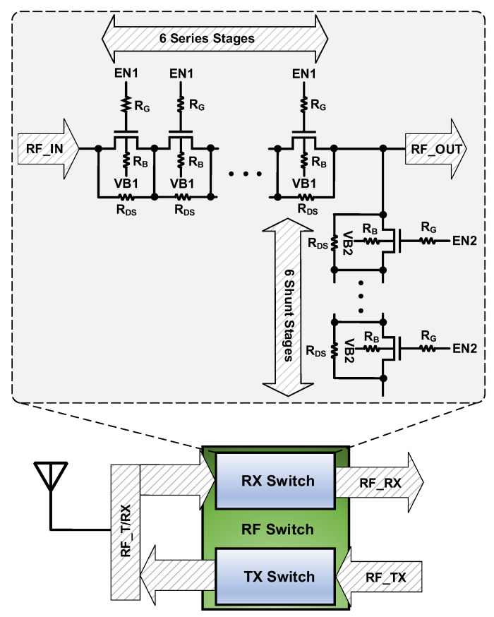
This paper presents a fast-switching Transmit/Receive (T/R) Single-Pole-Double-Throw (SPDT) Radio Frequency (RF) switch. Thorough analyses have been conducted to choose the optimum number of stacks, transistor sizes, gate and body voltages, to satisfy the required specifications. This switch applies six stacks of series and shunt transistors as big as 3.9 mm/160 nm and 0.75 mm/160 nm, respectively. A negative charge pump and a voltage booster generate the negative and boosted control voltages to improve the harmonics and to keep Inter-Modulation Distortion (IMD) performance of the switch over 100 dBc. A Low Drop-Out (LDO) regulator limits the boosted voltage in Absolute Maximum Rating (AMR) conditions and improves the switch performance for Process, Voltage and Temperature (PVT) variations. To reduce the size, a dense custom-made capacitor consisting of different types of capacitors has been presented where they have been placed over each other in layout considering the Design Rule Checks (DRC) and applied in negative charge pump, voltage booster and LDO. This switch has been fabricated and tested in a 90 nm Silicon-on-Insulator (SOI) process. The second and third IMD for all specified blockers remain over 100 dBc and the switching time as fast as 150 ns has been achieved. The Insertion Loss (IL) and isolation at 2.7 GHz are -0.17 dB and -33 dB, respectively. This design consumes 145 uA from supply voltage range of 1.65 V to 1.95 V and occupies 440 × 472 µm of die area.
本文介绍了一种快速切换的发射/接收(T/R)单刀双掷(SPDT)射频(RF)开关。已进行了全面分析,以选择最佳的堆叠数量、晶体管尺寸、栅极和体电压,以满足所需规格。该开关分别应用了六堆叠的串联和并联晶体管,尺寸分别为3.9 mm/160 nm和0.75 mm/160 nm。一个负电荷泵和一个电压升压器产生负控制电压和升压控制电压,以改善谐波,并使开关的互调失真(IMD)性能保持在100 dBc以上。一个低压差(LDO)调节器在绝对最大额定值(AMR)条件下限制升压电压,并改善开关在工艺、电压和温度(PVT)变化时的性能。为了减小尺寸,提出了一种由不同类型电容器组成的密集定制电容器,它们在布局中相互堆叠,并考虑了设计规则检查(DRC),应用于负电荷泵、电压升压器和LDO。该开关已在90 nm绝缘体上硅(SOI)工艺中制造和测试。对于所有指定的阻塞器,二次和三次IMD均保持在100 dBc以上,并且实现了最快150 ns的开关时间。在2.7 GHz时的插入损耗(IL)和隔离度分别为-0.17 dB和-33 dB。该设计在1.65 V至1.95 V的电源电压范围内消耗145 μA电流,占用440×472 µm的芯片面积。