Fang Y X, Zhang H, Azad F, Wang S P, Ling F C C, Su S C
Institute of Optoelectronic Material and Technology, South China Normal University Guangzhou 510631 P. R. China
School of Natural Sciences (SNS), National University of Sciences and Technology (NUST) H-12 Islamabad Pakistan.
RSC Adv. 2018 Aug 21;8(52):29555-29561. doi: 10.1039/c8ra05677c. eCollection 2018 Aug 20.
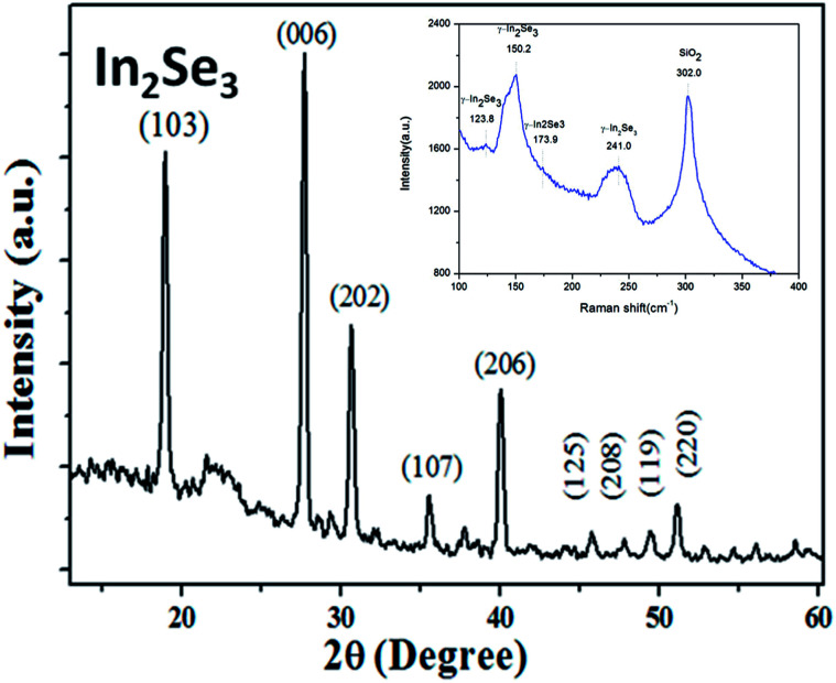
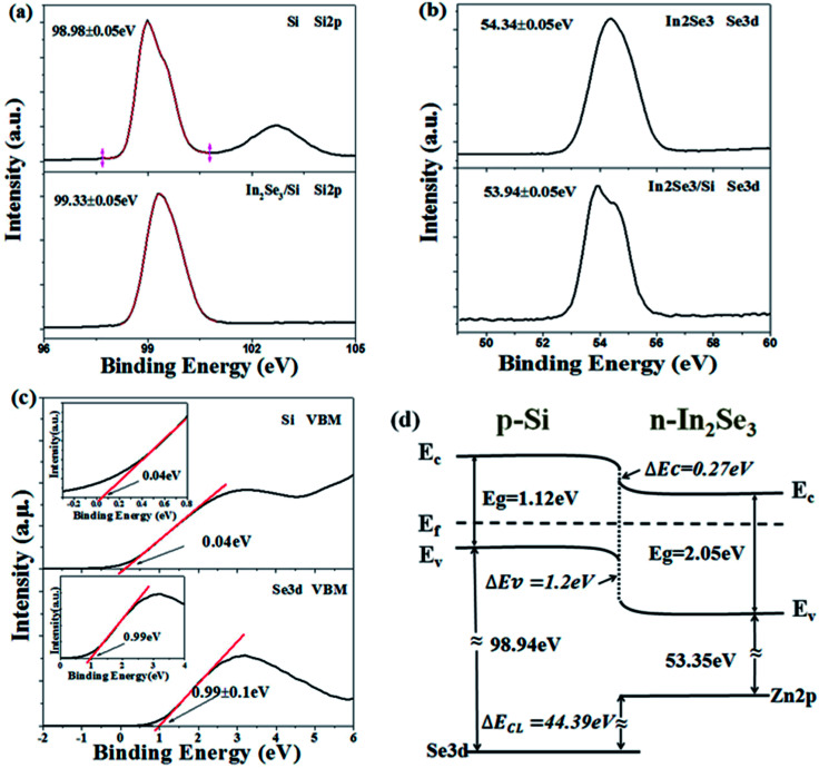
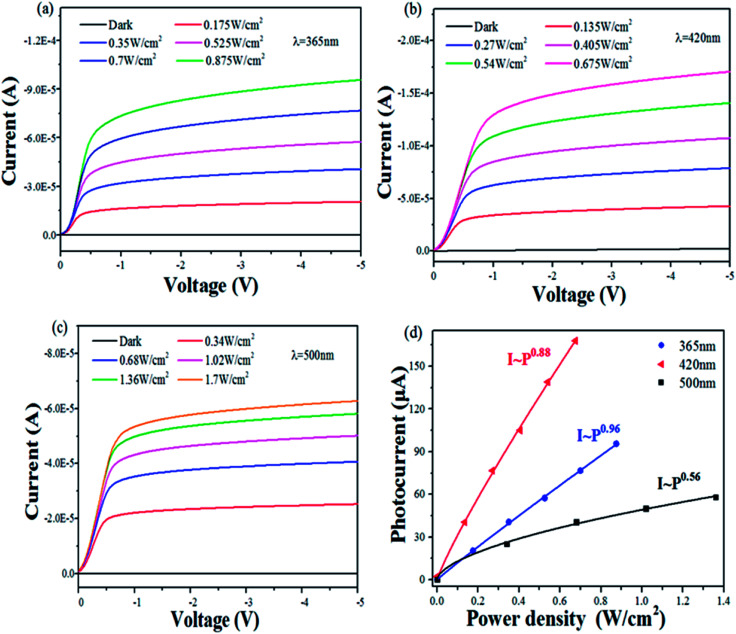
High-quality γ-InSe thin films and a γ-InSe/p-Si heterojunction were prepared using pulse laser deposition (PLD). The band offset of this heterojunction was studied by XPS and the band structure was found to be type II structure. The valence band offset (Δ ) and the conduction band offset (Δ ) of the heterojunction were determined to be 1.2 ± 0.1 eV and 0.27 ± 0.1 eV, respectively. The γ-InSe/p-Si heterojunction photodetector has high responsivity under UV to visible light illumination. The heterojunction exhibits highly stable photodetection characteristics with an ultrafast response/recovery time of 15/366 μs. The ultrafast response time was attributed to type II structure band alignment, which was good for the separation of electron-hole pairs and it can quickly reduce recombination. These excellent properties make γ-InSe/p-Si heterojunctions a promising candidate for photodetector applications.
采用脉冲激光沉积(PLD)制备了高质量的γ-InSe薄膜和γ-InSe/p-Si异质结。通过XPS研究了该异质结的带隙偏移,发现其能带结构为II型结构。该异质结的价带偏移(Δ )和导带偏移(Δ )分别确定为1.2±0.1 eV和0.27±0.1 eV。γ-InSe/p-Si异质结光电探测器在紫外到可见光照射下具有高响应度。该异质结表现出高度稳定的光电探测特性,超快响应/恢复时间为15/366 μs。超快响应时间归因于II型结构的能带排列,这有利于电子-空穴对的分离,并且可以快速减少复合。这些优异的特性使γ-InSe/p-Si异质结成为光电探测器应用的有前途的候选材料。