• 文献检索
  • 文档翻译
  • 深度研究
  • 学术资讯
  • Suppr Zotero 插件Zotero 插件
  • 邀请有礼
  • 套餐&价格
  • 历史记录
应用&插件
Suppr Zotero 插件Zotero 插件浏览器插件Mac 客户端Windows 客户端微信小程序
定价
高级版会员购买积分包购买API积分包
服务
文献检索文档翻译深度研究API 文档MCP 服务
关于我们
关于 Suppr公司介绍联系我们用户协议隐私条款
关注我们

Suppr 超能文献

核心技术专利:CN118964589B侵权必究
粤ICP备2023148730 号-1Suppr @ 2026

文献检索

告别复杂PubMed语法,用中文像聊天一样搜索,搜遍4000万医学文献。AI智能推荐,让科研检索更轻松。

立即免费搜索

文件翻译

保留排版,准确专业,支持PDF/Word/PPT等文件格式,支持 12+语言互译。

免费翻译文档

深度研究

AI帮你快速写综述,25分钟生成高质量综述,智能提取关键信息,辅助科研写作。

立即免费体验

金刚石纳米柱中NV中心系综的光学和自旋特性

Optical and Spin Properties of NV Center Ensembles in Diamond Nano-Pillars.

作者信息

Volkova Kseniia, Heupel Julia, Trofimov Sergei, Betz Fridtjof, Colom Rémi, MacQueen Rowan W, Akhundzada Sapida, Reginka Meike, Ehresmann Arno, Reithmaier Johann Peter, Burger Sven, Popov Cyril, Naydenov Boris

机构信息

Department Spins in Energy Conversion and Quantum Information Science (ASPIN), Helmholtz-Zentrum Berlin für Materialien und Energie GmbH, Hahn-Meitner-Platz 1, 14109 Berlin, Germany.

Institute of Nanostructure Technologies and Analytics (INA), Center for Interdisciplinary Nanostructure Science and Technology (CINSaT), University of Kassel, Heinrich-Plett-Str. 40, 34132 Kassel, Germany.

出版信息

Nanomaterials (Basel). 2022 Apr 29;12(9):1516. doi: 10.3390/nano12091516.

DOI:10.3390/nano12091516
PMID:35564222
原文链接:https://pmc.ncbi.nlm.nih.gov/articles/PMC9103819/
Abstract

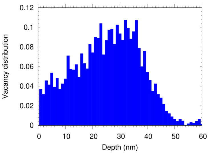
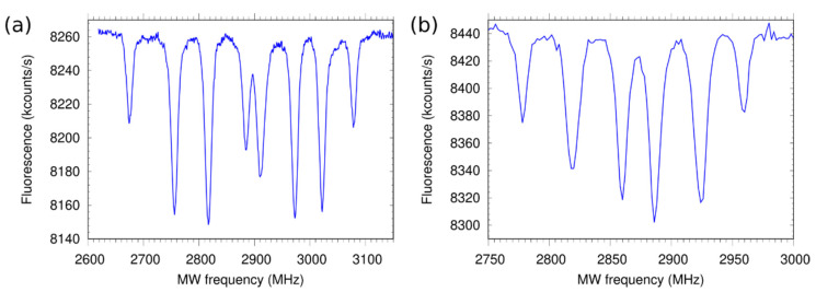
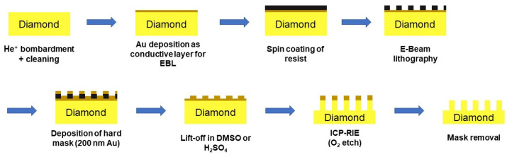
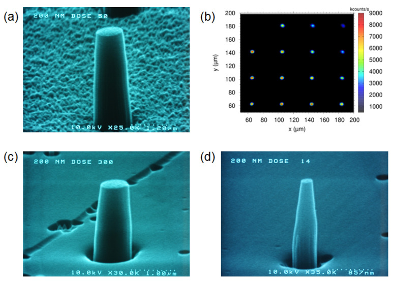
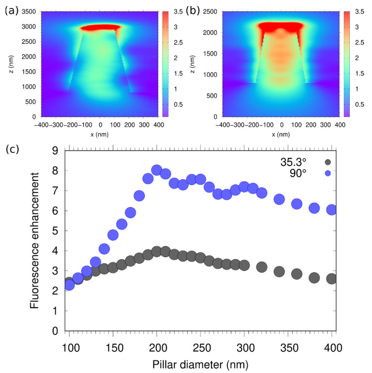
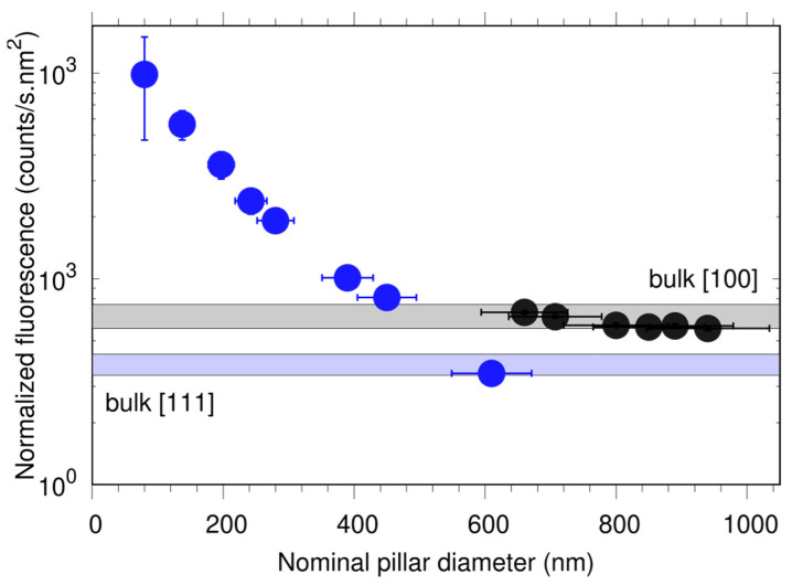
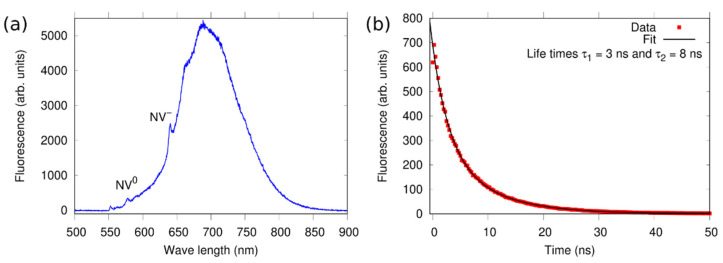
Nitrogen-vacancy (NV) color centers in diamond are excellent quantum sensors possessing high sensitivity and nano-scale spatial resolution. Their integration in photonic structures is often desired, since it leads to an increased photon emission and also allows the realization of solid-state quantum technology architectures. Here, we report the fabrication of diamond nano-pillars with diameters up to 1000 nm by electron beam lithography and inductively coupled plasma reactive ion etching in nitrogen-rich diamonds (type Ib) with [100] and [111] crystal orientations. The NV centers were created by keV-He ion bombardment and subsequent annealing, and we estimate an average number of NVs per pillar to be 4300 ± 300 and 520 ± 120 for the [100] and [111] samples, respectively. Lifetime measurements of the NVs' excited state showed two time constants with average values of τ ≈ 2 ns and τ ≈ 8 ns, which are shorter as compared to a single color center in a bulk crystal (τ ≈ 10 ns). This is probably due to a coupling between the NVs as well as due to interaction with bombardment-induced defects and substitutional nitrogen (P1 centers). Optically detected magnetic resonance measurements revealed a contrast of about 5% and average coherence and relaxation times of T [100] = 420 ± 40 ns, T [111] = 560 ± 50 ns, and T [100] = 162 ± 11 μs, T [111] = 174 ± 24 μs. These pillars could find an application for scanning probe magnetic field imaging.

摘要

金刚石中的氮空位(NV)色心是具有高灵敏度和纳米级空间分辨率的优秀量子传感器。人们常常希望将它们集成到光子结构中,因为这会增加光子发射,还能实现固态量子技术架构。在此,我们报告了通过电子束光刻和电感耦合等离子体反应离子刻蚀,在具有[100]和[111]晶体取向的富氮金刚石(Ib型)中制备直径达1000 nm的金刚石纳米柱。通过keV-He离子轰击和后续退火产生NV色心,我们估计[100]和[111]样品中每个纳米柱的NV平均数量分别为4300±300和520±120。对NV激发态的寿命测量显示出两个时间常数,平均值分别为τ≈2 ns和τ≈8 ns,与块状晶体中的单个色心(τ≈10 ns)相比更短。这可能是由于NV之间的耦合以及与轰击诱导的缺陷和替代氮(P1中心)的相互作用。光探测磁共振测量显示对比度约为5%,[100]的平均相干时间和弛豫时间为T[100]=420±40 ns,T[111]=560±50 ns,T[100]=162±11 μs,T[111]=174±24 μs。这些纳米柱可用于扫描探针磁场成像。

https://cdn.ncbi.nlm.nih.gov/pmc/blobs/99bd/9103819/b0a542c3f642/nanomaterials-12-01516-g007.jpg
https://cdn.ncbi.nlm.nih.gov/pmc/blobs/99bd/9103819/dfb8c6970281/nanomaterials-12-01516-g001.jpg
https://cdn.ncbi.nlm.nih.gov/pmc/blobs/99bd/9103819/dca4b3d1dd9b/nanomaterials-12-01516-g002.jpg
https://cdn.ncbi.nlm.nih.gov/pmc/blobs/99bd/9103819/5f9f33d238ea/nanomaterials-12-01516-g003.jpg
https://cdn.ncbi.nlm.nih.gov/pmc/blobs/99bd/9103819/d32b68b2a3db/nanomaterials-12-01516-g004.jpg
https://cdn.ncbi.nlm.nih.gov/pmc/blobs/99bd/9103819/32282bc2b635/nanomaterials-12-01516-g005.jpg
https://cdn.ncbi.nlm.nih.gov/pmc/blobs/99bd/9103819/3cb1a5d12d01/nanomaterials-12-01516-g006.jpg
https://cdn.ncbi.nlm.nih.gov/pmc/blobs/99bd/9103819/b0a542c3f642/nanomaterials-12-01516-g007.jpg

相似文献

1
Optical and Spin Properties of NV Center Ensembles in Diamond Nano-Pillars.金刚石纳米柱中NV中心系综的光学和自旋特性
Nanomaterials (Basel). 2022 Apr 29;12(9):1516. doi: 10.3390/nano12091516.
2
Nanoscale Engineering of Closely-Spaced Electronic Spins in Diamond.金刚石中紧密间隔电子自旋的纳米工程。
Nano Lett. 2016 Aug 10;16(8):4982-90. doi: 10.1021/acs.nanolett.6b01692. Epub 2016 Jul 21.
3
dc Magnetometry with Engineered Nitrogen-Vacancy Spin Ensembles in Diamond.利用金刚石中工程化氮空位自旋系综的直流磁强计。
Nano Lett. 2019 Sep 11;19(9):6681-6686. doi: 10.1021/acs.nanolett.9b02993. Epub 2019 Aug 27.
4
Fluorescent Nanodiamond: A Versatile Tool for Long-Term Cell Tracking, Super-Resolution Imaging, and Nanoscale Temperature Sensing.荧光纳米金刚石:用于长期细胞追踪、超分辨率成像和纳米级温度传感的多功能工具。
Acc Chem Res. 2016 Mar 15;49(3):400-7. doi: 10.1021/acs.accounts.5b00484. Epub 2016 Feb 16.
5
Toward Optimized Surface δ-Profiles of Nitrogen-Vacancy Centers Activated by Helium Irradiation in Diamond.氦离子辐照金刚石中氮空位中心的优化表面 δ 轮廓。
Nano Lett. 2016 Apr 13;16(4):2228-33. doi: 10.1021/acs.nanolett.5b04511. Epub 2016 Mar 4.
6
Nanoengineered diamond waveguide as a robust bright platform for nanomagnetometry using shallow nitrogen vacancy centers.纳米金刚石波导作为一个坚固的明亮平台,用于使用浅层氮空位中心的纳米磁力计。
Nano Lett. 2015 Jan 14;15(1):165-9. doi: 10.1021/nl503326t. Epub 2014 Dec 8.
7
Observing bulk diamond spin coherence in high-purity nanodiamonds.观察高纯纳米金刚石中的体金刚石自旋相干性。
Nat Mater. 2014 Jan;13(1):21-5. doi: 10.1038/nmat3805. Epub 2013 Nov 24.
8
Calibration-Free Vector Magnetometry Using Nitrogen-Vacancy Center in Diamond Integrated with Optical Vortex Beam.利用与光学涡旋光束集成的金刚石中的氮空位中心进行无校准矢量磁力测量。
Nano Lett. 2020 Nov 11;20(11):8267-8272. doi: 10.1021/acs.nanolett.0c03377. Epub 2020 Nov 2.
9
Nitrogen-vacancy-assisted magnetometry of paramagnetic centers in an individual diamond nanocrystal.氮空位辅助的单个金刚石纳米晶体中顺磁中心的磁强计。
Nano Lett. 2012 Jul 11;12(7):3477-82. doi: 10.1021/nl300964g. Epub 2012 Jun 28.
10
Hyperfine Interactions in the NV-C Quantum Registers in Diamond Grown from the Azaadamantane Seed.由氮杂金刚烷籽晶生长的金刚石中NV-C量子寄存器中的超精细相互作用。
Nanomaterials (Basel). 2021 May 14;11(5):1303. doi: 10.3390/nano11051303.

引用本文的文献

1
Coherent photoelectrical readout of single spins in silicon carbide at room temperature.室温下碳化硅中单个自旋的相干光电读出。
Nat Commun. 2025 Apr 15;16(1):3405. doi: 10.1038/s41467-025-58629-1.
2
Complex Three-Dimensional Microscale Structures for Quantum Sensing Applications.用于量子传感应用的复杂三维微尺度结构。
Nano Lett. 2023 Oct 25;23(20):9272-9279. doi: 10.1021/acs.nanolett.3c02251. Epub 2023 Oct 9.
3
Neuronal growth on high-aspect-ratio diamond nanopillar arrays for biosensing applications.用于生物传感应用的高纵横比金刚石纳米柱阵列上的神经元生长。

本文引用的文献

1
Enhanced Widefield Quantum Sensing with Nitrogen-Vacancy Ensembles Using Diamond Nanopillar Arrays.利用金刚石纳米柱阵列实现氮空位系综增强的宽场量子传感
ACS Appl Mater Interfaces. 2020 Mar 18;12(11):13421-13427. doi: 10.1021/acsami.9b19397. Epub 2020 Mar 6.
2
Deterministic placement of ultra-bright near-infrared color centers in arrays of silicon carbide micropillars.在碳化硅微柱阵列中确定性放置超亮近红外色心。
Beilstein J Nanotechnol. 2019 Dec 5;10:2383-2395. doi: 10.3762/bjnano.10.229. eCollection 2019.
3
Nanoengineered diamond waveguide as a robust bright platform for nanomagnetometry using shallow nitrogen vacancy centers.
Sci Rep. 2023 Apr 11;13(1):5909. doi: 10.1038/s41598-023-32235-x.
4
Templated Synthesis of Diamond Nanopillar Arrays Using Porous Anodic Aluminium Oxide (AAO) Membranes.使用多孔阳极氧化铝(AAO)膜模板法合成金刚石纳米柱阵列
Nanomaterials (Basel). 2023 Feb 27;13(5):888. doi: 10.3390/nano13050888.
5
Metal-Dielectric Nanopillar Antenna-Resonators for Efficient Collected Photon Rate from Silicon Carbide Color Centers.用于高效收集碳化硅色心光子速率的金属-电介质纳米柱天线谐振器
Nanomaterials (Basel). 2023 Jan 1;13(1):195. doi: 10.3390/nano13010195.
纳米金刚石波导作为一个坚固的明亮平台,用于使用浅层氮空位中心的纳米磁力计。
Nano Lett. 2015 Jan 14;15(1):165-9. doi: 10.1021/nl503326t. Epub 2014 Dec 8.
4
Magnetometry with nitrogen-vacancy defects in diamond.金刚石中的氮空位缺陷的磁力测量。
Rep Prog Phys. 2014 May;77(5):056503. doi: 10.1088/0034-4885/77/5/056503. Epub 2014 May 6.
5
Electronic properties and metrology applications of the diamond NV- center under pressure.压力下金刚石 NV-中心的电子性质和计量学应用。
Phys Rev Lett. 2014 Jan 31;112(4):047601. doi: 10.1103/PhysRevLett.112.047601.
6
Nanometre-scale thermometry in a living cell.活细胞中的纳米级测温。
Nature. 2013 Aug 1;500(7460):54-8. doi: 10.1038/nature12373.
7
High-precision nanoscale temperature sensing using single defects in diamond.利用金刚石中的单缺陷进行高精度纳米尺度温度传感。
Nano Lett. 2013 Jun 12;13(6):2738-42. doi: 10.1021/nl401216y.
8
Coupling of nitrogen-vacancy centers to photonic crystal cavities in monocrystalline diamond.氮空位中心与单晶金刚石中的光子晶体腔的耦合。
Phys Rev Lett. 2012 Jul 20;109(3):033604. doi: 10.1103/PhysRevLett.109.033604. Epub 2012 Jul 19.
9
A robust scanning diamond sensor for nanoscale imaging with single nitrogen-vacancy centres.一种用于单氮空位中心纳米成像的稳健扫描金刚石传感器。
Nat Nanotechnol. 2012 Apr 15;7(5):320-4. doi: 10.1038/nnano.2012.50.
10
Monolithic diamond optics for single photon detection.用于单光子探测的单片金刚石光学器件。
Appl Phys Lett. 2010 Dec 13;97(24):241902. doi: 10.1063/1.3519849.