Bieniek Maciej, Sadecka Katarzyna, Szulakowska Ludmiła, Hawrylak Paweł
Department of Physics, University of Ottawa, Ottawa, ON K1N 6N5, Canada.
Department of Theoretical Physics, Wrocław University of Science and Technology, Wybrzeże Wyspiańskiego 27, 50-370 Wrocław, Poland.
Nanomaterials (Basel). 2022 May 6;12(9):1582. doi: 10.3390/nano12091582.
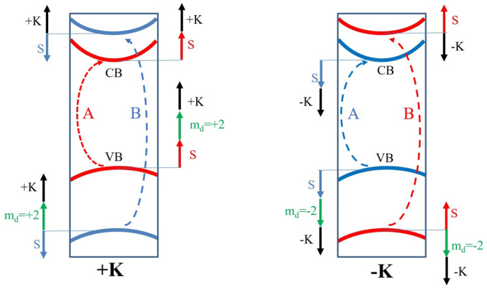
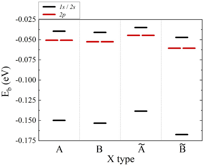
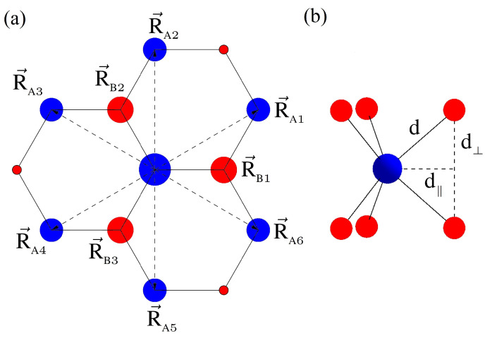
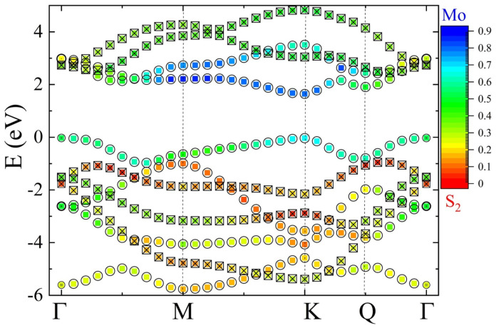
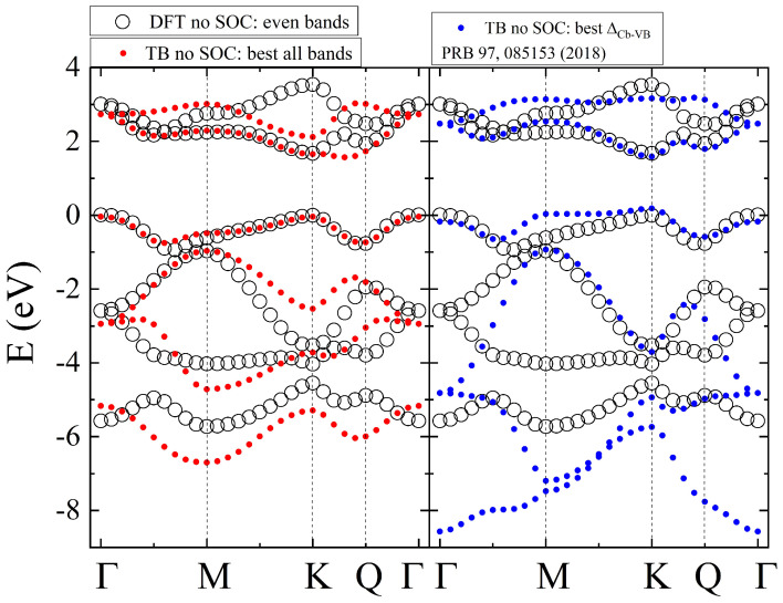
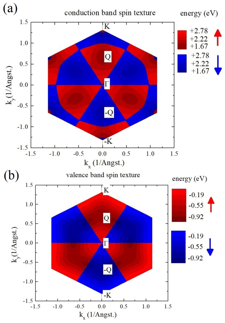
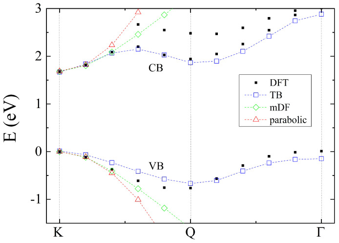
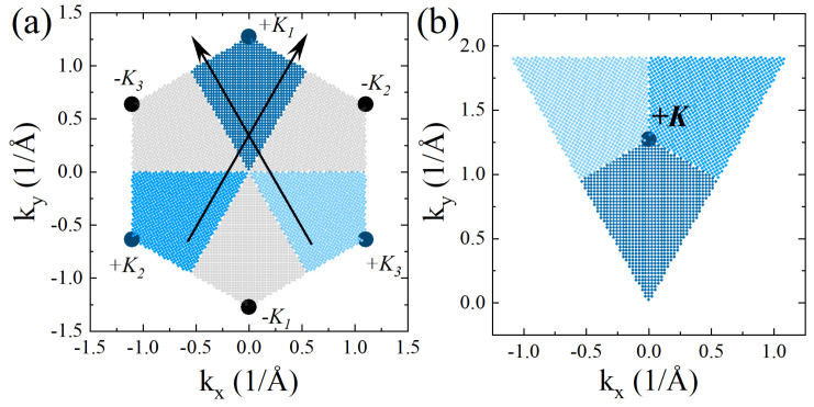
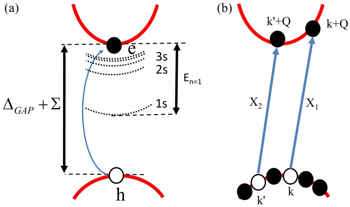
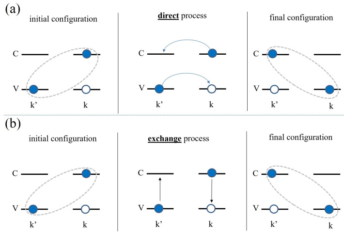
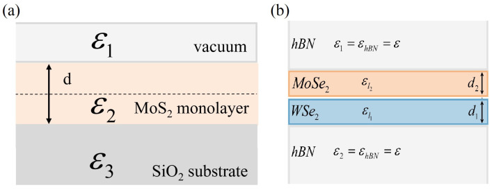
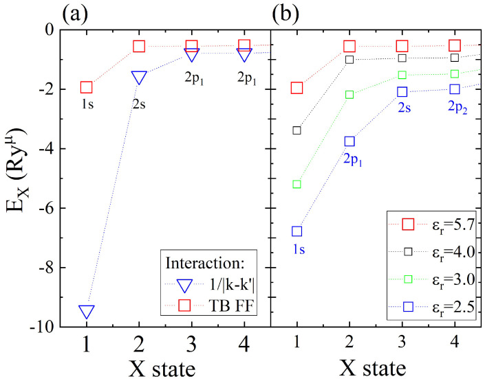
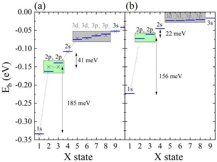
Atomically thin semiconductors from the transition metal dichalcogenide family are materials in which the optical response is dominated by strongly bound excitonic complexes. Here, we present a theory of excitons in two-dimensional semiconductors using a tight-binding model of the electronic structure. In the first part, we review extensive literature on 2D van der Waals materials, with particular focus on their optical response from both experimental and theoretical points of view. In the second part, we discuss our ab initio calculations of the electronic structure of MoS, representative of a wide class of materials, and review our minimal tight-binding model, which reproduces low-energy physics around the Fermi level and, at the same time, allows for the understanding of their electronic structure. Next, we describe how electron-hole pair excitations from the mean-field-level ground state are constructed. The electron-electron interactions mix the electron-hole pair excitations, resulting in excitonic wave functions and energies obtained by solving the Bethe-Salpeter equation. This is enabled by the efficient computation of the Coulomb matrix elements optimized for two-dimensional crystals. Next, we discuss non-local screening in various geometries usually used in experiments. We conclude with a discussion of the fine structure and excited excitonic spectra. In particular, we discuss the effect of band nesting on the exciton fine structure; Coulomb interactions; and the topology of the wave functions, screening and dielectric environment. Finally, we follow by adding another layer and discuss excitons in heterostructures built from two-dimensional semiconductors.
过渡金属二硫族化合物家族中的原子级薄半导体材料,其光学响应主要由强束缚激子复合体主导。在此,我们使用电子结构的紧束缚模型提出一种二维半导体激子理论。在第一部分,我们回顾了关于二维范德华材料的大量文献,特别从实验和理论角度关注其光学响应。在第二部分,我们讨论了对代表一类广泛材料的MoS电子结构的从头算计算,并回顾了我们的最小紧束缚模型,该模型再现了费米能级附近的低能物理现象,同时有助于理解其电子结构。接下来,我们描述了如何从平均场基态构建电子 - 空穴对激发。电子 - 电子相互作用混合了电子 - 空穴对激发,通过求解贝塞耳 - 萨尔彼得方程得到激子波函数和能量。这是通过对二维晶体优化的库仑矩阵元的高效计算实现的。接下来,我们讨论了实验中常用的各种几何结构中的非局部屏蔽。我们以对精细结构和激发激子光谱的讨论作为结论。特别是,我们讨论了能带嵌套对激子精细结构的影响;库仑相互作用;以及波函数的拓扑结构、屏蔽和介电环境。最后,我们通过添加另一层来讨论由二维半导体构建的异质结构中的激子。