• 文献检索
  • 文档翻译
  • 深度研究
  • 学术资讯
  • Suppr Zotero 插件Zotero 插件
  • 邀请有礼
  • 套餐&价格
  • 历史记录
应用&插件
Suppr Zotero 插件Zotero 插件浏览器插件Mac 客户端Windows 客户端微信小程序
定价
高级版会员购买积分包购买API积分包
服务
文献检索文档翻译深度研究API 文档MCP 服务
关于我们
关于 Suppr公司介绍联系我们用户协议隐私条款
关注我们

Suppr 超能文献

核心技术专利:CN118964589B侵权必究
粤ICP备2023148730 号-1Suppr @ 2026

文献检索

告别复杂PubMed语法,用中文像聊天一样搜索,搜遍4000万医学文献。AI智能推荐,让科研检索更轻松。

立即免费搜索

文件翻译

保留排版,准确专业,支持PDF/Word/PPT等文件格式,支持 12+语言互译。

免费翻译文档

深度研究

AI帮你快速写综述,25分钟生成高质量综述,智能提取关键信息,辅助科研写作。

立即免费体验

复杂硅碳结构的制造:探索碳化硅材料

Manufacturing of Complex Silicon-Carbon Structures: Exploring SiC Materials.

作者信息

Oglesby Skyler, Ivanov Sergei A, Londonõ-Calderon Alejandra, Pete Douglas, Pettes Michael Thompson, Jones Andrew Crandall, Chabi Sakineh

机构信息

Department of Mechanical Engineering, University of New Mexico, Albuquerque, NM 87131, USA.

Materials Physics and Application Division, Los Alamos National Laboratory, Los Alamos, NM 87545, USA.

出版信息

Materials (Basel). 2022 May 12;15(10):3475. doi: 10.3390/ma15103475.

DOI:10.3390/ma15103475
PMID:35629503
原文链接:https://pmc.ncbi.nlm.nih.gov/articles/PMC9146070/
Abstract

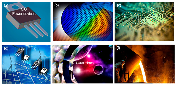
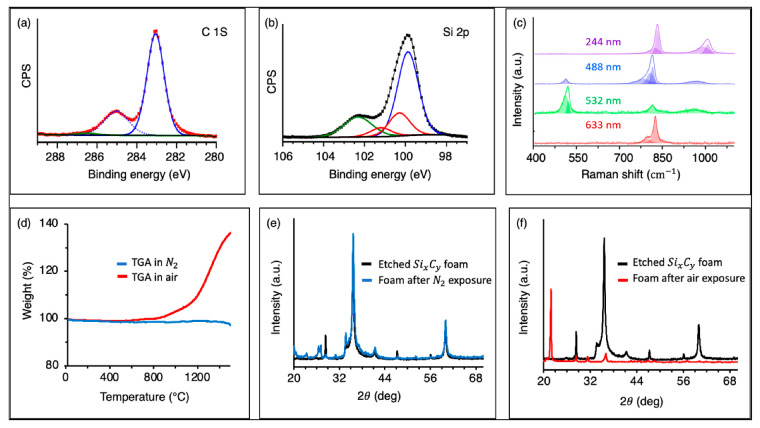
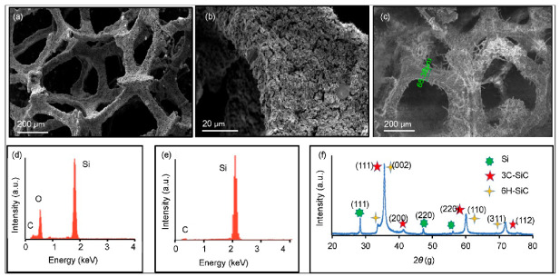
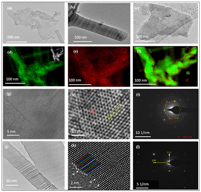
This paper reports on the manufacturing of complex three-dimensional Si/C structures via a chemical vapor deposition method. The structure and properties of the grown materials were characterized using various techniques including scanning electron microscopy, aberration-corrected transmission electron microscopy, confocal Raman spectroscopy, and X-ray photoelectron spectroscopy. The spectroscopy results revealed that the grown materials were composed of micro/nanostructures with various compositions and dimensions. These included two-dimensional silicon carbide (SiC), cubic silicon, and various SiC polytypes. The coexistence of these phases at the nano-level and their interfaces can benefit several Si/C-based applications ranging from ceramics and structural applications to power electronics, aerospace, and high-temperature applications. With an average density of 7 mg/cm, the grown materials can be considered ultralightweight, as they are three orders of magnitude lighter than bulk Si/C materials. This study aims to impact how ceramic materials are manufactured, which may lead to the design of new carbide materials or Si/C-based lightweight structures with additional functionalities and desired properties.

摘要

本文报道了通过化学气相沉积法制造复杂三维硅碳结构的过程。使用包括扫描电子显微镜、像差校正透射电子显微镜、共焦拉曼光谱和X射线光电子能谱在内的各种技术对生长材料的结构和性能进行了表征。光谱结果表明,生长材料由具有不同组成和尺寸的微/纳米结构组成。这些结构包括二维碳化硅(SiC)、立方硅和各种SiC多型体。这些相在纳米级的共存及其界面有利于多种基于硅碳的应用,从陶瓷和结构应用到电力电子、航空航天和高温应用。生长材料的平均密度为7 mg/cm,可被视为超轻材料,因为它们比块状硅碳材料轻三个数量级。本研究旨在影响陶瓷材料的制造方式,这可能会导致设计出具有附加功能和所需性能的新型碳化物材料或基于硅碳的轻质结构。

https://cdn.ncbi.nlm.nih.gov/pmc/blobs/b538/9146070/f32fd3102b92/materials-15-03475-g004.jpg
https://cdn.ncbi.nlm.nih.gov/pmc/blobs/b538/9146070/3454066b3f59/materials-15-03475-g001.jpg
https://cdn.ncbi.nlm.nih.gov/pmc/blobs/b538/9146070/d21d3207a508/materials-15-03475-g002.jpg
https://cdn.ncbi.nlm.nih.gov/pmc/blobs/b538/9146070/77e633cd5a3f/materials-15-03475-g003.jpg
https://cdn.ncbi.nlm.nih.gov/pmc/blobs/b538/9146070/f32fd3102b92/materials-15-03475-g004.jpg

相似文献

1
Manufacturing of Complex Silicon-Carbon Structures: Exploring SiC Materials.复杂硅碳结构的制造:探索碳化硅材料
Materials (Basel). 2022 May 12;15(10):3475. doi: 10.3390/ma15103475.
2
Two-Dimensional Silicon Carbide: Emerging Direct Band Gap Semiconductor.二维碳化硅:新兴的直接带隙半导体
Nanomaterials (Basel). 2020 Nov 9;10(11):2226. doi: 10.3390/nano10112226.
3
Silicon carbide embedded in carbon nanofibres: structure and band gap determination.嵌入碳纳米纤维中的碳化硅:结构与带隙测定
Phys Chem Chem Phys. 2014 Nov 28;16(44):24437-42. doi: 10.1039/c4cp02975e.
4
Homogeneous nanocrystalline cubic silicon carbide films prepared by inductively coupled plasma chemical vapor deposition.通过电感耦合等离子体化学气相沉积制备的均匀纳米晶立方碳化硅薄膜。
Nanotechnology. 2007 Nov 21;18(46):465601. doi: 10.1088/0957-4484/18/46/465601. Epub 2007 Oct 12.
5
Crystal structures and the electronic properties of silicon-rich silicon carbide materials by first principle calculations.通过第一性原理计算研究富硅碳化硅材料的晶体结构和电子性质
Heliyon. 2019 Nov 27;5(11):e02908. doi: 10.1016/j.heliyon.2019.e02908. eCollection 2019 Nov.
6
Extended vapor-liquid-solid growth of silicon carbide nanowires.碳化硅纳米线的扩展气-液-固生长
J Nanosci Nanotechnol. 2014 Apr;14(4):2741-51. doi: 10.1166/jnn.2014.8569.
7
The Creation of True Two-Dimensional Silicon Carbide.真二维碳化硅的制备
Nanomaterials (Basel). 2021 Jul 10;11(7):1799. doi: 10.3390/nano11071799.
8
Low energy Si, SiCH, or C beam injections to silicon substrates during chemical vapor deposition with dimethylsilane.在使用二甲基硅烷进行化学气相沉积期间,向硅衬底注入低能量的硅、硅碳或碳束。
Heliyon. 2023 Aug 6;9(8):e19002. doi: 10.1016/j.heliyon.2023.e19002. eCollection 2023 Aug.
9
XPS analysis by exclusion of a-carbon layer on silicon carbide nanowires by a gold catalyst-supported metal-organic chemical vapor deposition method.通过金催化剂负载的金属有机化学气相沉积法排除碳化硅纳米线上的α-碳层进行X射线光电子能谱分析。
J Nanosci Nanotechnol. 2010 Apr;10(4):2741-5. doi: 10.1166/jnn.2010.1384.
10
Ceramic Composite Materials Obtained by Electron-Beam Physical Vapor Deposition Used as Thermal Barriers in the Aerospace Industry.通过电子束物理气相沉积获得的陶瓷复合材料在航空航天工业中用作热障。
Nanomaterials (Basel). 2020 Feb 20;10(2):370. doi: 10.3390/nano10020370.

引用本文的文献

1
Effective Polarizability in Near-Field Microscopy of Phonon-Polariton Resonances.声子极化激元共振近场显微镜中的有效极化率
Nanomaterials (Basel). 2025 Mar 18;15(6):458. doi: 10.3390/nano15060458.

本文引用的文献

1
Recent progress in silk fibroin-based flexible electronics.基于丝素蛋白的柔性电子学的最新进展。
Microsyst Nanoeng. 2021 May 6;7:35. doi: 10.1038/s41378-021-00261-2. eCollection 2021.
2
The Creation of True Two-Dimensional Silicon Carbide.真二维碳化硅的制备
Nanomaterials (Basel). 2021 Jul 10;11(7):1799. doi: 10.3390/nano11071799.
3
Materials challenges and opportunities for quantum computing hardware.量子计算硬件面临的材料挑战与机遇
Science. 2021 Apr 16;372(6539). doi: 10.1126/science.abb2823.
4
Graphene and two-dimensional materials for silicon technology.用于硅技术的石墨烯和二维材料。
Nature. 2019 Sep;573(7775):507-518. doi: 10.1038/s41586-019-1573-9. Epub 2019 Sep 25.
5
Versatile mechanical properties of novel g-SiC monolayers from graphene to silicene: a first-principles study.从石墨烯到硅烯的新型g-SiC单层的多功能力学性能:第一性原理研究
Nanotechnology. 2018 Aug 3;29(31):315701. doi: 10.1088/1361-6528/aac337. Epub 2018 May 9.
6
Nanolattices: An Emerging Class of Mechanical Metamaterials.纳米晶格:一类新兴的力学超材料。
Adv Mater. 2017 Oct;29(40). doi: 10.1002/adma.201701850. Epub 2017 Sep 5.
7
SiC7 siligraphene: a novel donor material with extraordinary sunlight absorption.碳化硅7硅石墨烯:一种具有非凡阳光吸收能力的新型供体材料。
Nanoscale. 2016 Apr 7;8(13):6994-9. doi: 10.1039/c6nr00046k.
8
Ultralight, Strong, Three-Dimensional SiC Structures.超轻、高强的三维碳化硅结构
ACS Nano. 2016 Feb 23;10(2):1871-6. doi: 10.1021/acsnano.5b05533. Epub 2015 Nov 23.
9
Origin of Dirac Cones in SiC Silagraphene: A Combined Density Functional and Tight-Binding Study.碳化硅硅石墨烯中狄拉克锥的起源:密度泛函与紧束缚联合研究
J Phys Chem Lett. 2015 Apr 16;6(8):1333-9. doi: 10.1021/acs.jpclett.5b00365. Epub 2015 Mar 27.
10
Innovation economics. Where is Silicon Valley?创新经济学。硅谷在哪里?
Science. 2015 Feb 6;347(6222):606-9. doi: 10.1126/science.aaa0201. Epub 2015 Feb 5.