Institute for Applied Microelectronics (IUMA), Departament of Electronics and Automatic Engineering, University of Las Palmas de Gran Canaria (ULPGC), Campus Universitario de Tafira, 35017 Las Palmas de Gran Canaria, Spain.
Instituto de Astrofísica de Canarias (IAC), 38205 San Cristóbal de La Laguna, Spain.
Sensors (Basel). 2022 Jul 13;22(14):5246. doi: 10.3390/s22145246.
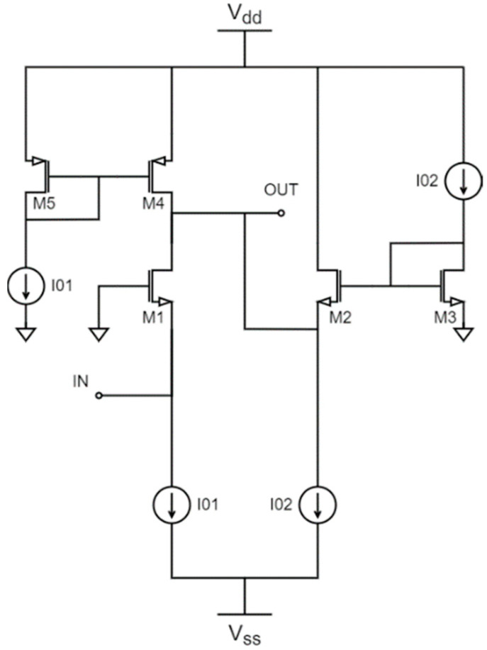
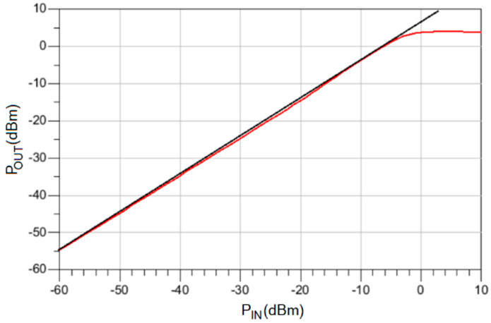
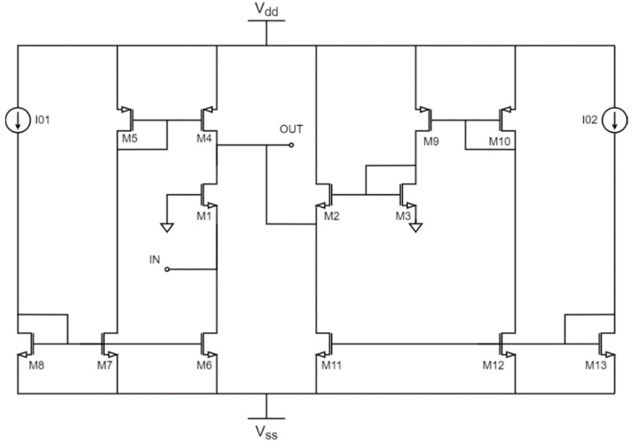
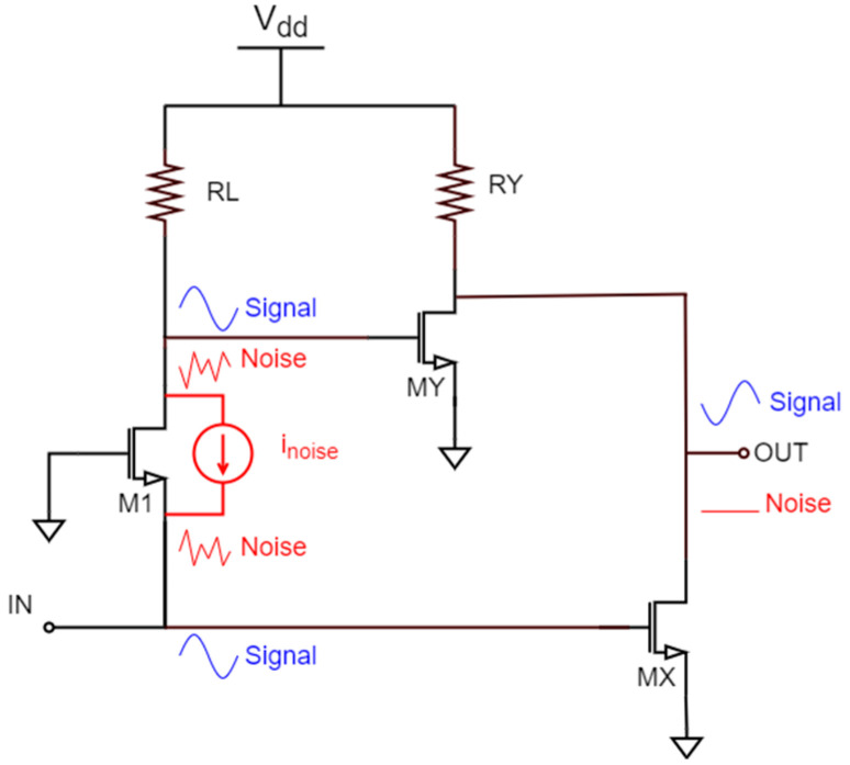
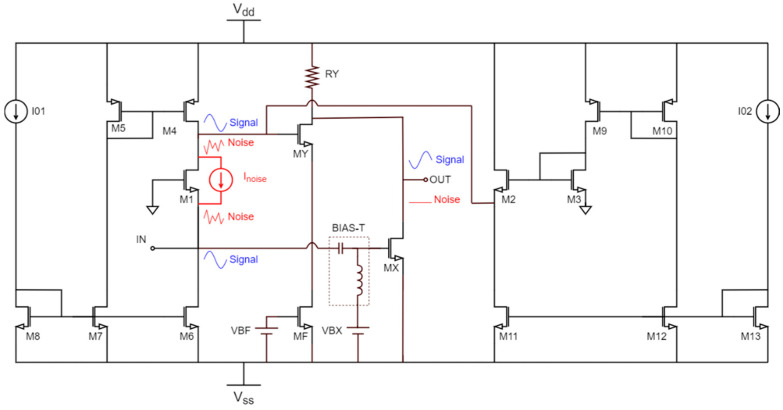
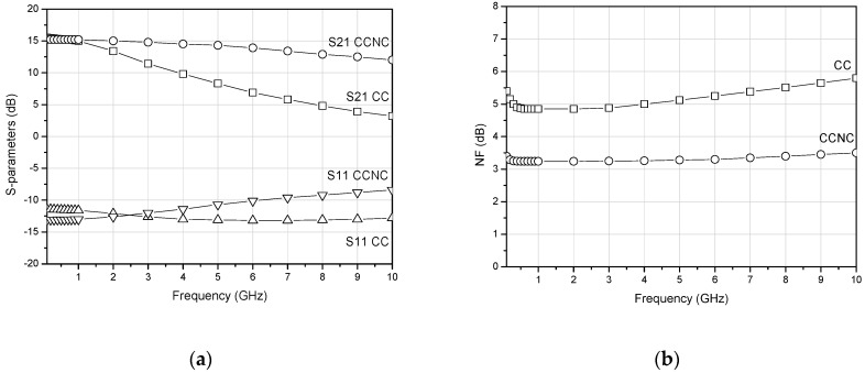
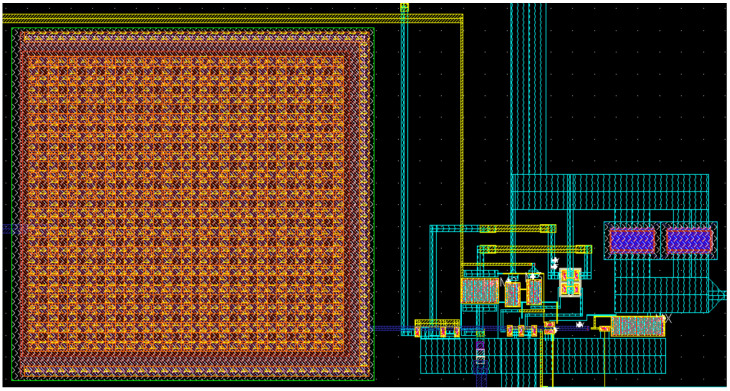
In this paper, a wide-band noise-canceling (NC) current conveyor (CC)-based CMOS low-noise amplifier (LNA) is presented. The circuit employs a CC-based approach to obtain wide-band input matching without the need for bulky inductances, allowing broadband performance with a very small area used. The NC technique is applied by subtracting the input transistor’s noise contribution to the output and achieves a noise figure (NF) reduction from 4.8 dB to 3.2 dB. The NC LNA is implemented in a UMC 65-nm CMOS process and occupies an area of only 160 × 80 μm2. It achieves a stable frequency response from 0 to 6.2 GHz, a maximum gain of 15.3 dB, an input return loss (S11) < −10 dB, and a remarkable IIP3 of 7.6 dBm, while consuming 18.6 mW from a ±1.2 V DC supply. Comparisons with similar works prove the effectiveness of this new implementation, showing that the circuit obtains a noteworthy performance trade-off.
本文提出了一种基于宽频噪声消除(NC)电流传输器(CC)的 CMOS 低噪声放大器(LNA)。该电路采用基于 CC 的方法实现宽带输入匹配,无需使用庞大的电感,从而在占用极小面积的情况下实现宽带性能。通过从输出端减去输入晶体管的噪声贡献,应用 NC 技术可将噪声系数(NF)从 4.8 dB 降低至 3.2 dB。该 NC LNA 采用 UMC 65nm CMOS 工艺实现,面积仅为 160×80μm2。它在 0 至 6.2GHz 范围内实现稳定的频率响应,最大增益为 15.3dB,输入回波损耗(S11)<-10dB,IIP3 高达 7.6dBm,同时仅需 ±1.2V 直流电源供电 18.6mW。与类似工作的比较证明了这种新实现的有效性,表明该电路实现了显著的性能折衷。