Dibos Alan M, Solomon Michael T, Sullivan Sean E, Singh Manish K, Sautter Kathryn E, Horn Connor P, Grant Gregory D, Lin Yulin, Wen Jianguo, Heremans F Joseph, Guha Supratik, Awschalom David D
Nanoscience and Technology Division, Argonne National Laboratory, Lemont, Illinois 60439, United States.
Center for Molecular Engineering, Argonne National Laboratory, Lemont, Illinois 60439, United States.
Nano Lett. 2022 Aug 24;22(16):6530-6536. doi: 10.1021/acs.nanolett.2c01561. Epub 2022 Aug 8.
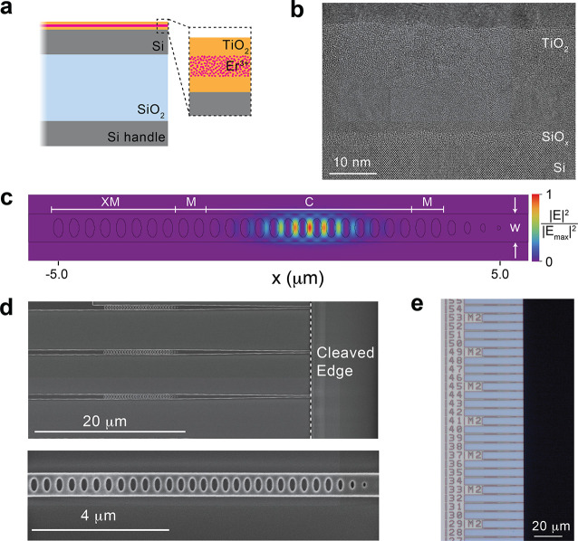
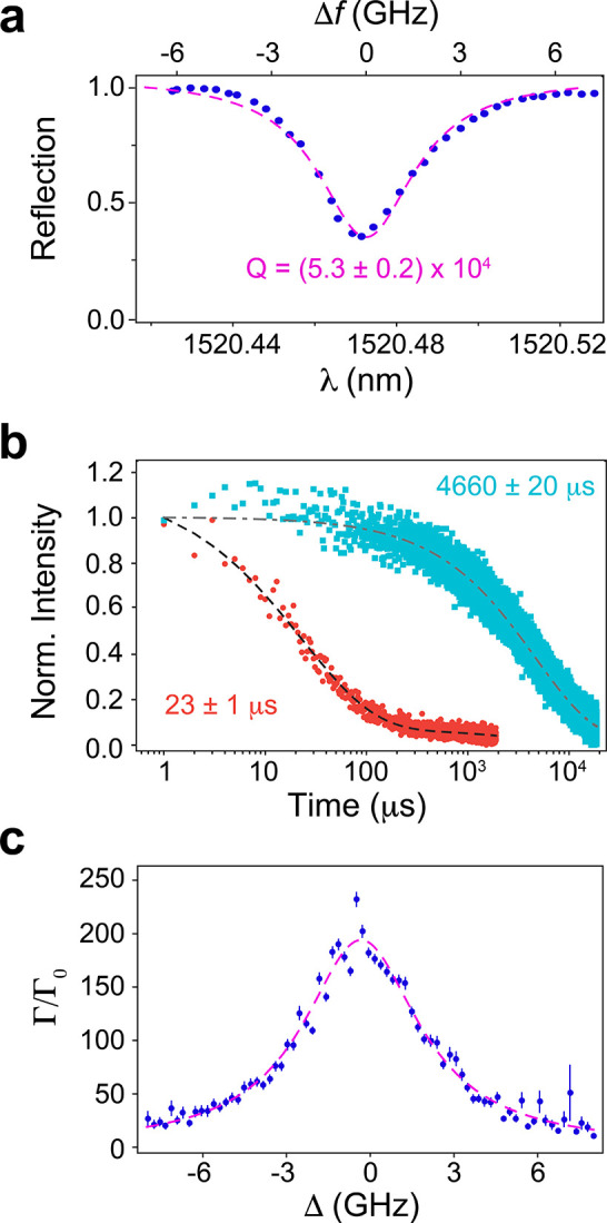
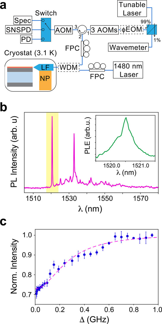
Isolated solid-state atomic defects with telecom optical transitions are ideal quantum photon emitters and spin qubits for applications in long-distance quantum communication networks. Prototypical telecom defects, such as erbium, suffer from poor photon emission rates, requiring photonic enhancement using resonant optical cavities. Moreover, many of the traditional hosts for erbium ions are not amenable to direct incorporation with existing integrated photonics platforms, limiting scalable fabrication of qubit-based devices. Here, we present a scalable approach toward CMOS-compatible telecom qubits by using erbium-doped titanium dioxide thin films grown atop silicon-on-insulator substrates. From this heterostructure, we have fabricated one-dimensional photonic crystal cavities demonstrating quality factors in excess of 5 × 10 and corresponding Purcell-enhanced optical emission rates of the erbium ensembles in excess of 200. This easily fabricated materials platform represents an important step toward realizing telecom quantum memories in a scalable qubit architecture compatible with mature silicon technologies.
具有电信光跃迁的孤立固态原子缺陷是长距离量子通信网络应用中理想的量子光子发射器和自旋量子比特。典型的电信缺陷,如铒,光子发射率较低,需要使用共振光学腔进行光子增强。此外,许多传统的铒离子宿主不易直接与现有的集成光子平台结合,限制了基于量子比特的器件的可扩展制造。在这里,我们通过在绝缘体上硅衬底上生长掺铒二氧化钛薄膜,提出了一种实现与CMOS兼容的电信量子比特的可扩展方法。从这种异质结构中,我们制造了一维光子晶体腔,其品质因数超过5×10,铒系综相应的珀塞尔增强光发射率超过200。这种易于制造的材料平台是朝着在与成熟硅技术兼容的可扩展量子比特架构中实现电信量子存储器迈出的重要一步。