Watanabe Kazuyoshi, Miura Naoki, Taguchi Hiroaki, Komatsu Takeshi, Nosaka Hideyuki, Okamoto Toshihiro, Watanabe Shun, Takeya Jun
Department of Advanced Materials Science, Graduate School of Frontier Sciences, The University of Tokyo, 5-1-5 Kashiwanoha, Kashiwa, Chiba, 277-8561, Japan.
NTT Device Technology Laboratories, Nippon Telegraph and Telephone (NTT) Corporation, 3-1 Morinosato-Wakamiya, Atsugi, Kanagawa, 243-0198, Japan.
Sci Rep. 2022 Oct 7;12(1):16009. doi: 10.1038/s41598-022-19387-y.
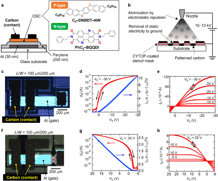
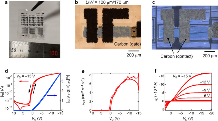
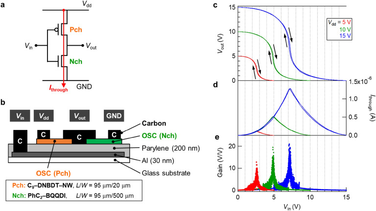
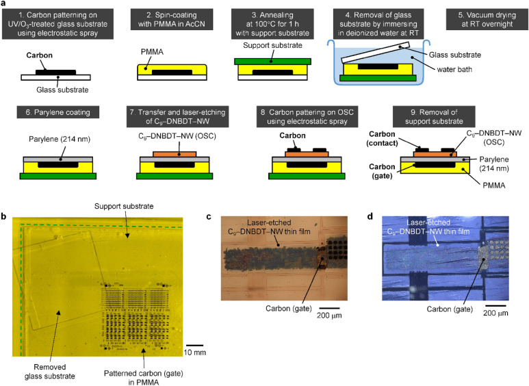
Organic thin-film transistors (OTFTs) are promising building blocks of flexible printable electronic devices. Similar to inorganic FETs, OTFTs are heterostructures consisting of metals, insulators, and semiconductors, in which nanoscale interfaces between different components should be precisely engineered. However, OTFTs use noble metals, such as gold, as electrodes, which has been a bottleneck in terms of cost reduction and low environmental loading. In this study, we demonstrate that graphite-based carbon electrodes can be deposited and patterned directly onto an organic single-crystalline thin film via electrostatic spray coating. The present OTFTs exhibited reasonably high field-effect mobilities of up to 11 cm V s for p-type and 1.4 cm V s for n-type with no significant deterioration during electrostatic spray processes. We also demonstrate two significant milestones from the viewpoint of material science: a complementary circuit, an inverter consisting of p- and n-type OTFTs, and an operatable metal-free OTFT composed of fully carbon-based materials. These results constitute a key step forward in the further development of printed metal-free integrated circuits.
有机薄膜晶体管(OTFT)是柔性可印刷电子设备中很有前景的构建模块。与无机场效应晶体管类似,OTFT是由金属、绝缘体和半导体组成的异质结构,其中不同组件之间的纳米级界面需要精确设计。然而,OTFT使用金等贵金属作为电极,这在降低成本和低环境负荷方面一直是个瓶颈。在本研究中,我们证明了基于石墨的碳电极可以通过静电喷涂直接沉积并图案化在有机单晶薄膜上。目前的OTFT表现出相当高的场效应迁移率,p型高达11 cm² V⁻¹ s⁻¹,n型为1.4 cm² V⁻¹ s⁻¹,在静电喷涂过程中没有明显劣化。从材料科学的角度来看,我们还展示了两个重要的里程碑:一个互补电路,一个由p型和n型OTFT组成的反相器,以及一个由完全基于碳的材料组成的可操作无金属OTFT。这些结果是进一步开发印刷无金属集成电路的关键一步。