• 文献检索
  • 文档翻译
  • 深度研究
  • 学术资讯
  • Suppr Zotero 插件Zotero 插件
  • 邀请有礼
  • 套餐&价格
  • 历史记录
应用&插件
Suppr Zotero 插件Zotero 插件浏览器插件Mac 客户端Windows 客户端微信小程序
定价
高级版会员购买积分包购买API积分包
服务
文献检索文档翻译深度研究API 文档MCP 服务
关于我们
关于 Suppr公司介绍联系我们用户协议隐私条款
关注我们

Suppr 超能文献

核心技术专利:CN118964589B侵权必究
粤ICP备2023148730 号-1Suppr @ 2026

文献检索

告别复杂PubMed语法,用中文像聊天一样搜索,搜遍4000万医学文献。AI智能推荐,让科研检索更轻松。

立即免费搜索

文件翻译

保留排版,准确专业,支持PDF/Word/PPT等文件格式,支持 12+语言互译。

免费翻译文档

深度研究

AI帮你快速写综述,25分钟生成高质量综述,智能提取关键信息,辅助科研写作。

立即免费体验

低损耗垂直TiO/聚合物混合纳米波导

Low Loss Vertical TiO/Polymer Hybrid Nano-Waveguides.

作者信息

Doughan Isaac, Oyemakinwa Kehinde, Ovaskainen Olli, Roussey Matthieu

机构信息

Department of Physics and Mathematics, Center for Photonics Sciences, University of Eastern Finland, P.O. Box 111, 80101 Joensuu, Finland.

出版信息

Nanomaterials (Basel). 2023 Jan 24;13(3):469. doi: 10.3390/nano13030469.

DOI:10.3390/nano13030469
PMID:36770429
原文链接:https://pmc.ncbi.nlm.nih.gov/articles/PMC9921058/
Abstract

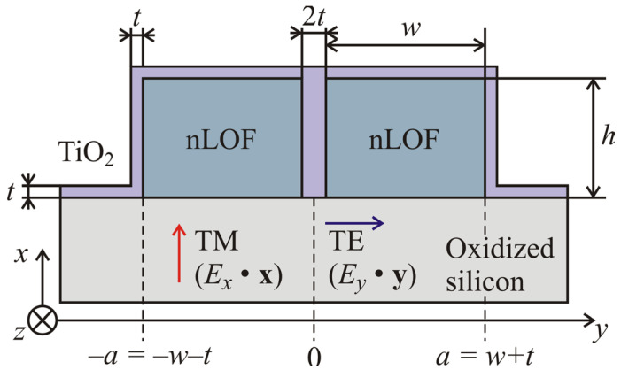
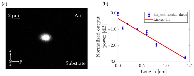
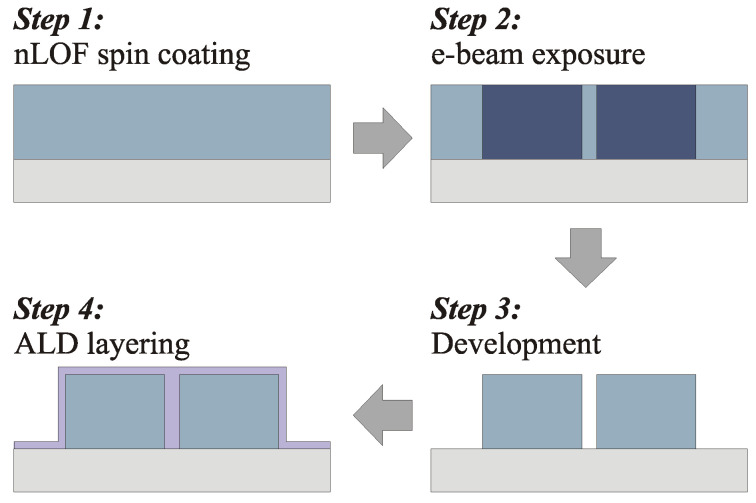
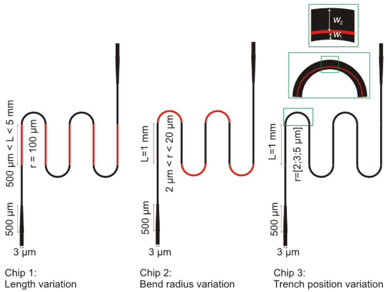
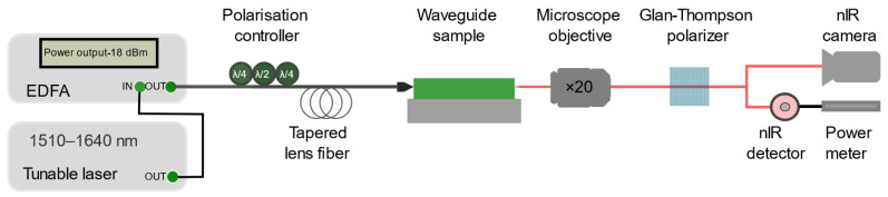
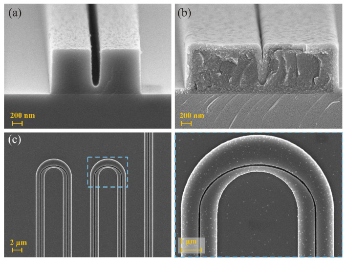
This article proposes a novel demonstration of a low-loss polymer channel hybridized with a titania core leading to a nano-waveguide elongated in the normal direction to the substrate. It is aimed at using the quasi-transverse magnetic (TM) mode as the predominant mode in compact photonic circuitry. A detailed design analysis shows how a thin layer of a higher-refractive index material in a trench within the core of the waveguide can increase the confinement and reduce the propagation losses. This thin layer, produced by atomic layer deposition, covers the entire polymer structure in a conformal manner, ensuring both a reduction of the surface roughness and a stronger field confinement. The trench can be made at any place within the polymer channel and therefore its position can be tuned to obtain asymmetric modal distribution. The waveguide is demonstrated at telecom wavelengths, although the material's properties enable operation over a large part of the electromagnetic spectrum. We measured propagation losses as low as 1.75 ± 0.32 dB/cm in a 200 nm × 900 nm section of the waveguide core. All processes being mass-production compatible, this study opens a path towards easier integrated-component manufacture.

摘要

本文提出了一种新型的低损耗聚合物通道,它与二氧化钛芯相结合,形成了一个沿垂直于衬底方向延伸的纳米波导。其目的是在紧凑型光子电路中使用准横磁(TM)模式作为主要模式。详细的设计分析表明,波导芯内沟槽中的一层高折射率材料薄层如何能够增加光场限制并降低传播损耗。通过原子层沉积制备的这一薄层以共形方式覆盖整个聚合物结构,既确保了表面粗糙度的降低,又实现了更强的场限制。沟槽可以在聚合物通道内的任何位置形成,因此其位置可以进行调整以获得不对称的模式分布。尽管该材料的特性使其能够在大部分电磁频谱范围内工作,但该波导是在电信波长下进行演示的。我们在波导芯200 nm×900 nm的截面中测得传播损耗低至1.75±0.32 dB/cm。由于所有工艺都与大规模生产兼容,这项研究为更易于制造集成组件开辟了一条道路。

https://cdn.ncbi.nlm.nih.gov/pmc/blobs/52d6/9921058/7bfa875cfd37/nanomaterials-13-00469-g009.jpg
https://cdn.ncbi.nlm.nih.gov/pmc/blobs/52d6/9921058/a698ede3dc00/nanomaterials-13-00469-g001.jpg
https://cdn.ncbi.nlm.nih.gov/pmc/blobs/52d6/9921058/e3449775b092/nanomaterials-13-00469-g002.jpg
https://cdn.ncbi.nlm.nih.gov/pmc/blobs/52d6/9921058/663f0bf4eaa1/nanomaterials-13-00469-g003.jpg
https://cdn.ncbi.nlm.nih.gov/pmc/blobs/52d6/9921058/c0231df68f05/nanomaterials-13-00469-g004.jpg
https://cdn.ncbi.nlm.nih.gov/pmc/blobs/52d6/9921058/fe36d7ff9e39/nanomaterials-13-00469-g005.jpg
https://cdn.ncbi.nlm.nih.gov/pmc/blobs/52d6/9921058/4a50cd3c7bb8/nanomaterials-13-00469-g006.jpg
https://cdn.ncbi.nlm.nih.gov/pmc/blobs/52d6/9921058/0cb5a755868c/nanomaterials-13-00469-g007.jpg
https://cdn.ncbi.nlm.nih.gov/pmc/blobs/52d6/9921058/328ff85dc4c7/nanomaterials-13-00469-g008.jpg
https://cdn.ncbi.nlm.nih.gov/pmc/blobs/52d6/9921058/7bfa875cfd37/nanomaterials-13-00469-g009.jpg

相似文献

1
Low Loss Vertical TiO/Polymer Hybrid Nano-Waveguides.低损耗垂直TiO/聚合物混合纳米波导
Nanomaterials (Basel). 2023 Jan 24;13(3):469. doi: 10.3390/nano13030469.
2
2D optical confinement in an etchless stratified trench waveguide.无刻蚀分层脊形波导中的二维光学限制。
Opt Express. 2023 Feb 13;31(4):5140-5154. doi: 10.1364/OE.466004.
3
Waveguides consisting of single-crystal lithium niobate thin film and oxidized titanium stripe.由单晶硅酸锂薄膜和氧化钛条纹组成的波导。
Opt Express. 2015 Sep 21;23(19):24212-9. doi: 10.1364/OE.23.024212.
4
High-confinement alumina waveguides with sub-dB/cm propagation losses at 450 nm.在450纳米波长下具有低于1分贝/厘米传播损耗的高限制氧化铝波导。
Sci Rep. 2023 Nov 14;13(1):19917. doi: 10.1038/s41598-023-46877-4.
5
Strip-loaded horizontal slot waveguide.带状加载水平缝隙波导。
Opt Lett. 2017 Jan 15;42(2):211-214. doi: 10.1364/OL.42.000211.
6
Impact of ALD grown passivation layers on silicon nitride based integrated optic devices for very-near-infrared wavelengths.原子层沉积生长的钝化层对用于极近红外波长的氮化硅基集成光学器件的影响。
Opt Express. 2014 Mar 10;22(5):5684-92. doi: 10.1364/OE.22.005684.
7
Low bend loss femtosecond laser written waveguides exploiting integrated microcrack.利用集成微裂纹的低弯曲损耗飞秒激光写入波导
Sci Rep. 2021 Dec 9;11(1):23770. doi: 10.1038/s41598-021-03116-y.
8
Low-loss amorphous silicon wire waveguide for integrated photonics: effect of fabrication process and the thermal stability.用于集成光子学的低损耗非晶硅线波导:制造工艺的影响及热稳定性
Opt Express. 2010 Nov 22;18(24):25283-91. doi: 10.1364/OE.18.025283.
9
Thermal tuning of graphene-embedded waveguide filters based on the polymer-silica hybrid structure.基于聚合物-二氧化硅混合结构的石墨烯嵌入式波导滤波器的热调谐
RSC Adv. 2018 Aug 31;8(54):30755-30760. doi: 10.1039/c8ra06038j. eCollection 2018 Aug 30.
10
Mode Sensitivity Exploration of Silica-Titania Waveguide for Refractive Index Sensing Applications.用于折射率传感应用的硅钛酸盐波导的模式灵敏度探索。
Sensors (Basel). 2021 Nov 9;21(22):7452. doi: 10.3390/s21227452.

引用本文的文献

1
Determination of mode strengths in channel waveguide from the complex electric field.基于复电场确定通道波导中的模式强度
Sci Rep. 2024 Nov 19;14(1):28665. doi: 10.1038/s41598-024-80054-5.
2
Strip-loaded Mach-Zehnder interferometer for absolute refractive index sensing.用于绝对折射率传感的条形加载马赫-曾德尔干涉仪。
Sci Rep. 2024 Feb 6;14(1):3064. doi: 10.1038/s41598-024-53326-3.

本文引用的文献

1
Polarization Control in Integrated Silicon Waveguides Using Semiconductor Nanowires.使用半导体纳米线的集成硅波导中的偏振控制
Nanomaterials (Basel). 2022 Jul 16;12(14):2438. doi: 10.3390/nano12142438.
2
CuO/PMMA Polymer Nanocomposites as Novel Resist Materials for E-Beam Lithography.氧化铜/聚甲基丙烯酸甲酯聚合物纳米复合材料作为电子束光刻的新型抗蚀剂材料
Nanomaterials (Basel). 2021 Mar 17;11(3):762. doi: 10.3390/nano11030762.
3
Development of low-loss TiO waveguides.低损耗TiO光波导的开发。
Opt Express. 2020 Mar 2;28(5):5982-5990. doi: 10.1364/OE.380793.
4
Oblique incidence of semi-guided planar waves on slab waveguide steps: effects of rounded edges.平板波导阶跃处半引导平面波的斜入射:圆角的影响。
Opt Express. 2018 Jul 9;26(14):18621-18632. doi: 10.1364/OE.26.018621.
5
Atomic Layer Deposition of Silicon Nitride Thin Films: A Review of Recent Progress, Challenges, and Outlooks.氮化硅薄膜的原子层沉积:近期进展、挑战与展望综述
Materials (Basel). 2016 Dec 12;9(12):1007. doi: 10.3390/ma9121007.
6
Strip-loaded horizontal slot waveguide.带状加载水平缝隙波导。
Opt Lett. 2017 Jan 15;42(2):211-214. doi: 10.1364/OL.42.000211.
7
Low-loss titanium dioxide waveguides and resonators using a dielectric lift-off fabrication process.采用介电层剥离制造工艺的低损耗二氧化钛波导和谐振器。
Opt Express. 2015 May 4;23(9):11160-9. doi: 10.1364/OE.23.011160.
8
Design and optimization of waveguide sensitivity in slot microring sensors.狭缝微环传感器中波导灵敏度的设计与优化
J Opt Soc Am A Opt Image Sci Vis. 2011 Apr 1;28(4):596-603. doi: 10.1364/JOSAA.28.000596.
9
Modal characteristics of antiresonant reflecting pipe waveguides for terahertz waveguiding.用于太赫兹波导的反谐振反射管波导的模态特性
Opt Express. 2010 Jan 4;18(1):309-22. doi: 10.1364/OE.18.000309.
10
Accurate analysis of planar optical waveguide devices using higher-order FDTD scheme.使用高阶有限时域差分法对平面光波导器件进行精确分析。
Opt Express. 2006 Nov 27;14(24):11796-803. doi: 10.1364/oe.14.011796.