Department of Chemistry, Center for BioAnalytical Chemistry, Key Laboratory of Bioorganic Phosphorus Chemistry & Chemical Biology of Ministry of Education, Tsinghua University, Beijing, 100084, China.
State Key Laboratory of Molecular Reaction Dynamics, Dalian Institute of Chemical Physics, Chinese Academy of Sciences, Dalian, 116023, China.
Adv Sci (Weinh). 2023 May;10(13):e2206560. doi: 10.1002/advs.202206560. Epub 2023 Feb 25.
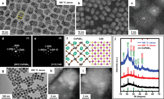
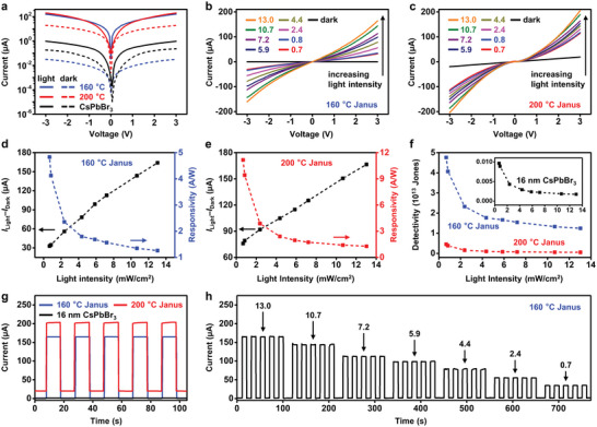
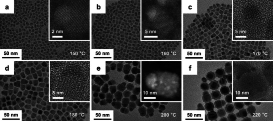
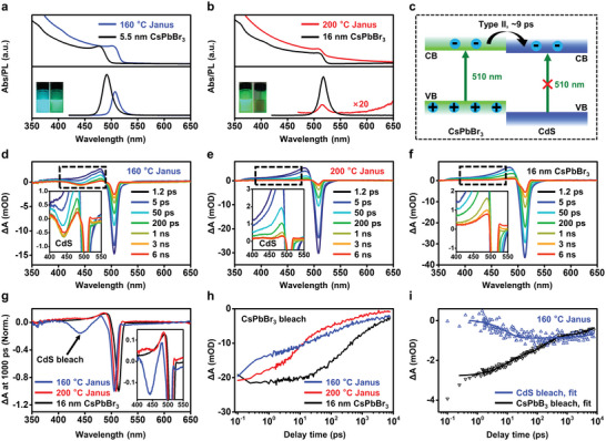
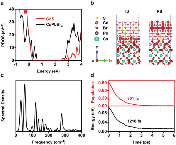
Epitaxial heterostructures of colloidal lead halide perovskite nanocrystals (NCs) with other semiconductors, especially the technologically important metal chalcogenides, can offer an unprecedented level of control in wavefunction design and exciton/charge carrier engineering. These NC heterostructures are ideal material platforms for efficient optoelectronics and other applications. Existing methods, however, can only yield heterostructures with random connections and distributions of the two components. The lack of epitaxial relation and uniform geometry hinders the structure-function correlation and impedes the electronic coupling at the heterointerface. This work reports the synthesis of uniform, epitaxially grown CsPbBr /CdS Janus NC heterostructures with ultrafast charge separation across the electronically coupled interface. Each Janus NC contains a CdS domain that grows exclusively on a single {220} facet of CsPbBr NCs. Varying reaction parameters allows for precise control in the sizes of each domain and readily modulates the optical properties of Janus NCs. Transient absorption measurements and modeling results reveal a type II band alignment, where photoexcited electrons rapidly transfer (within ≈9 picoseconds) from CsPbBr to CdS. The promoted charge separation and extraction in epitaxial Janus NCs leads to photoconductors with drastically improved (approximately three orders of magnitude) responsivity and detectivity, which is promising for ultrasensitive photodetection.
胶体铅卤钙钛矿纳米晶体(NCs)与其他半导体,特别是技术上重要的金属硫属化物的外延异质结构,可以在波函数设计和激子/电荷载流子工程方面提供前所未有的控制水平。这些 NC 异质结构是高效光电和其他应用的理想材料平台。然而,现有的方法只能得到两种成分具有随机连接和分布的异质结构。缺乏外延关系和均匀的几何形状阻碍了结构-功能相关性,并阻碍了异质界面处的电子耦合。这项工作报道了均匀的外延生长 CsPbBr/CdS 单一半导体 NC 异质结构的合成,该异质结构在电子耦合界面上具有超快的电荷分离。每个单一半导体 NC 都包含一个 CdS 畴,它仅在 CsPbBr NC 的单个{220}面上生长。通过改变反应参数,可以精确控制每个畴的大小,并容易地调节单一半导体 NC 的光学性质。瞬态吸收测量和建模结果表明存在 II 型能带排列,其中光激发电子从 CsPbBr 快速转移(在 ≈9 皮秒内)到 CdS。在外延单一半导体 NC 中促进的电荷分离和提取导致光电导性大大提高(约三个数量级),响应度和探测率,这对于超灵敏光电探测具有很大的应用前景。