Li Shuo, Francaviglia Luca, Kohler Daniel D, Jones Zachary R, Zhao Eric T, Ogletree D Frank, Weber-Bargioni Alexander, Melosh Nicholas A, Hamers Robert J
Department of Chemistry, University of Wisconsin-Madison, 1101 University Avenue, Madison, Wisconsin 53706, United States.
Stanford Institute for Materials and Energy Sciences, SLAC National Accelerator Laboratory, Menlo Park, California 94025, United States.
ACS Mater Au. 2021 Oct 22;2(2):85-93. doi: 10.1021/acsmaterialsau.1c00027. eCollection 2022 Mar 9.
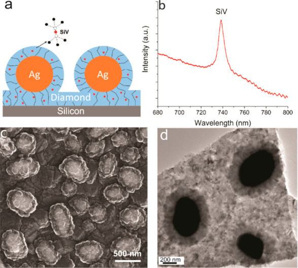
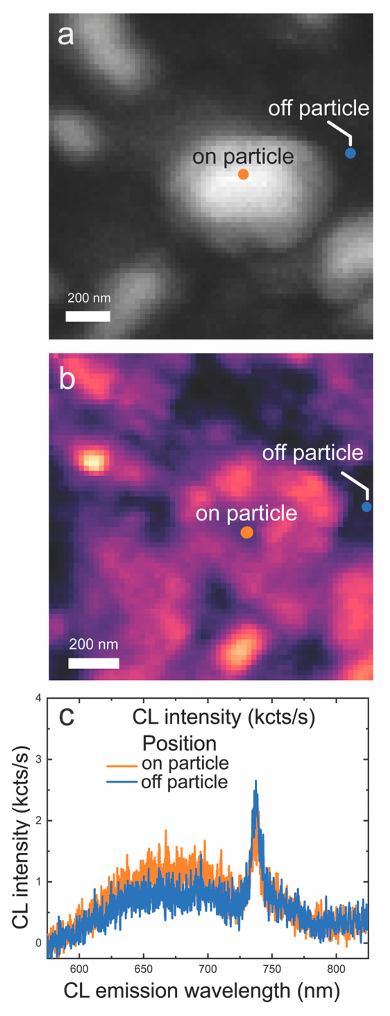
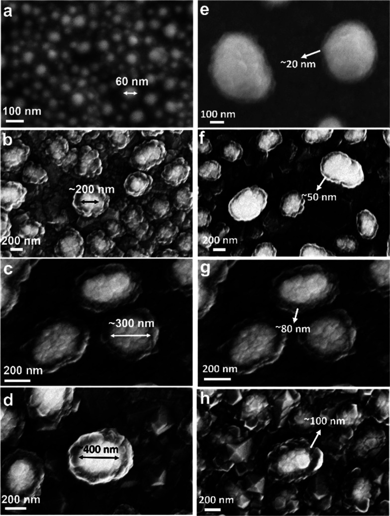
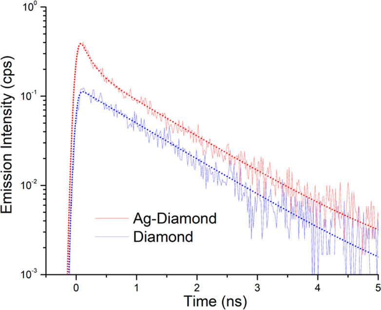
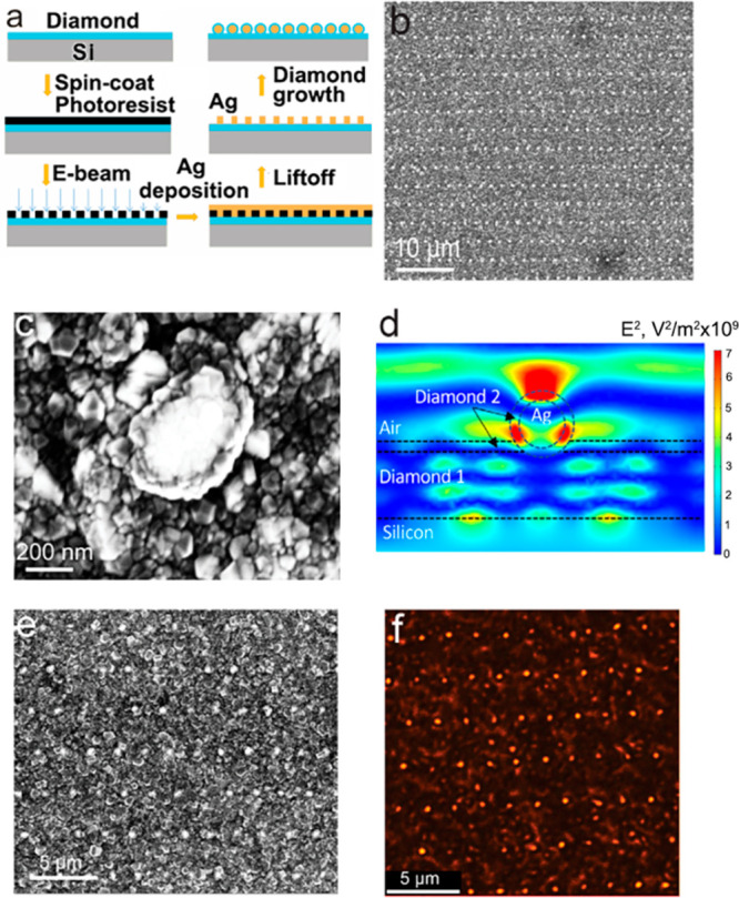
Silicon-vacancy (SiV) centers in diamond have attracted attention as highly stable fluorophores for sensing and as possible candidates for quantum information science. While prior studies have shown that the formation of hybrid diamond-metal structures can increase the rates of optical absorption and emission, many practical applications require diamond plasmonic structures that are stable in harsh chemical and thermal environments. Here, we demonstrate that Ag nanospheres, produced both in quasi-random arrays by thermal dewetting and in ordered arrays using electron-beam lithography, can be completely encapsulated with a thin diamond coating containing SiV centers, leading to hybrid core-shell nanostructures exhibiting extraordinary chemical and thermal stability as well as enhanced optical properties. Diamond shells with a thickness on the order of 20-100 nm are sufficient to encapsulate and protect the Ag nanostructures with different sizes ranging from 20 nm to hundreds of nanometers, allowing them to withstand heating to temperatures of 1000 °C and immersion in harsh boiling acid for 24 h. Ultrafast photoluminescence lifetime and super-resolution optical imaging experiments were used to study the SiV properties on and off the core-shell structures, which show that the SiV on core-shell structures have higher brightness and faster decay rate. The stability and optical properties of the hybrid Ag-diamond core-shell structures make them attractive candidates for high-efficiency imaging and quantum-based sensing applications.
金刚石中的硅空位(SiV)中心作为用于传感的高度稳定荧光团以及量子信息科学的潜在候选者受到了关注。虽然先前的研究表明,混合金刚石-金属结构的形成可以提高光吸收和发射速率,但许多实际应用需要在苛刻的化学和热环境中稳定的金刚石等离子体结构。在这里,我们证明,通过热去湿以准随机阵列形式制备以及使用电子束光刻以有序阵列形式制备的银纳米球,可以被含有SiV中心的薄金刚石涂层完全包裹,从而形成具有非凡化学和热稳定性以及增强光学性质的混合核壳纳米结构。厚度约为20-100nm的金刚石壳足以包裹和保护尺寸从20nm到数百纳米不等的不同银纳米结构,使其能够承受加热到1000°C的温度并在强沸腾酸中浸泡24小时。超快光致发光寿命和超分辨率光学成像实验被用于研究核壳结构上和核壳结构外的SiV特性,结果表明核壳结构上的SiV具有更高的亮度和更快的衰减率。混合银-金刚石核壳结构的稳定性和光学性质使其成为高效成像和基于量子的传感应用的有吸引力的候选者。