• 文献检索
  • 文档翻译
  • 深度研究
  • 学术资讯
  • Suppr Zotero 插件Zotero 插件
  • 邀请有礼
  • 套餐&价格
  • 历史记录
应用&插件
Suppr Zotero 插件Zotero 插件浏览器插件Mac 客户端Windows 客户端微信小程序
定价
高级版会员购买积分包购买API积分包
服务
文献检索文档翻译深度研究API 文档MCP 服务
关于我们
关于 Suppr公司介绍联系我们用户协议隐私条款
关注我们

Suppr 超能文献

核心技术专利:CN118964589B侵权必究
粤ICP备2023148730 号-1Suppr @ 2026

文献检索

告别复杂PubMed语法,用中文像聊天一样搜索,搜遍4000万医学文献。AI智能推荐,让科研检索更轻松。

立即免费搜索

文件翻译

保留排版,准确专业,支持PDF/Word/PPT等文件格式,支持 12+语言互译。

免费翻译文档

深度研究

AI帮你快速写综述,25分钟生成高质量综述,智能提取关键信息,辅助科研写作。

立即免费体验

载流子陷阱及其对氮化铝镓/氮化镓纳米线环绕栅晶体管表面和核心的影响。

Carrier Trap and Their Effects on the Surface and Core of AlGaN/GaN Nanowire Wrap-Gate Transistor.

作者信息

Mallem Siva Pratap Reddy, Puneetha Peddathimula, Lee Dong-Yeon, Kim Yoonkap, Kim Han-Jung, Im Ki-Sik, An Sung-Jin

机构信息

Advanced Material Research Center, Kumoh National Institute of Technology, Gumi 39177, Republic of Korea.

Department of Robotics and Intelligent Machine Engineering, College of Mechanical and IT Engineering, Yeungnam University, Gyeongsan 38541, Republic of Korea.

出版信息

Nanomaterials (Basel). 2023 Jul 22;13(14):2132. doi: 10.3390/nano13142132.

DOI:10.3390/nano13142132
PMID:37513143
原文链接:https://pmc.ncbi.nlm.nih.gov/articles/PMC10386025/
Abstract

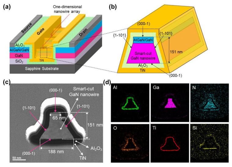
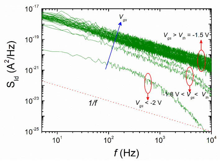
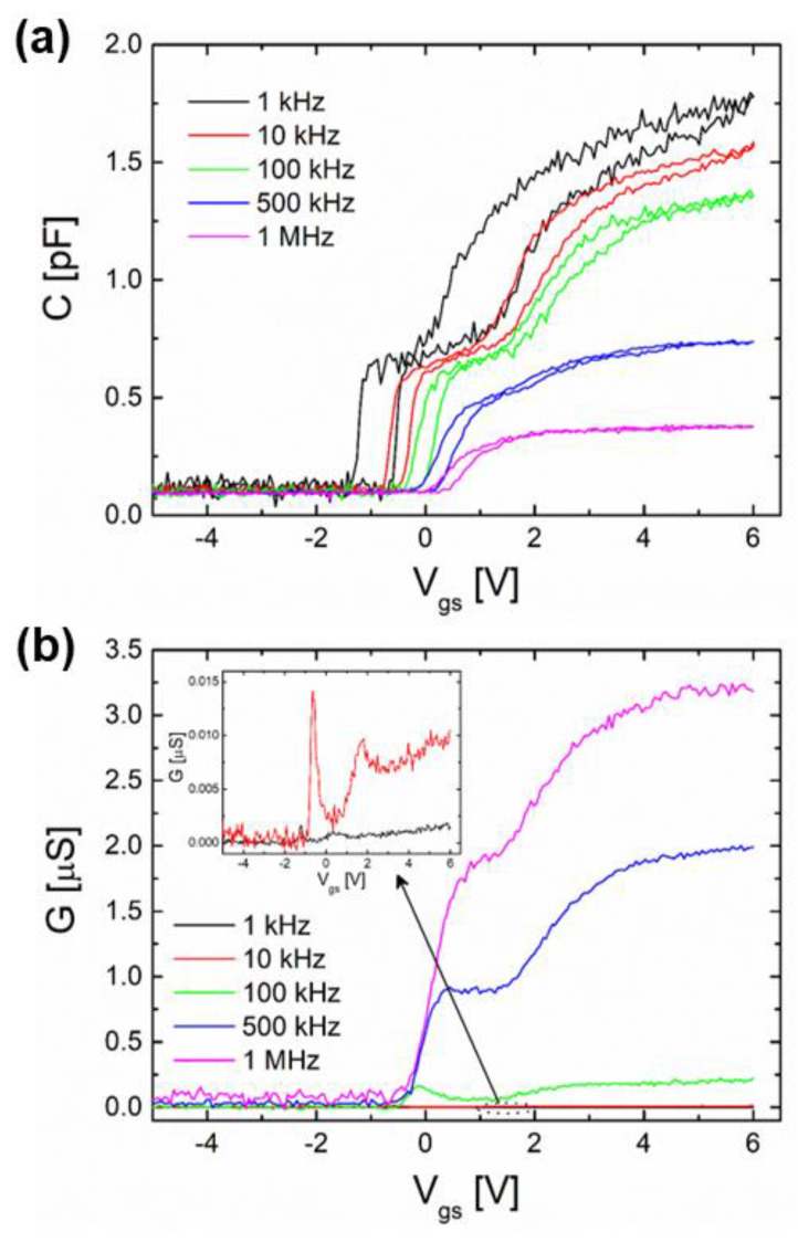
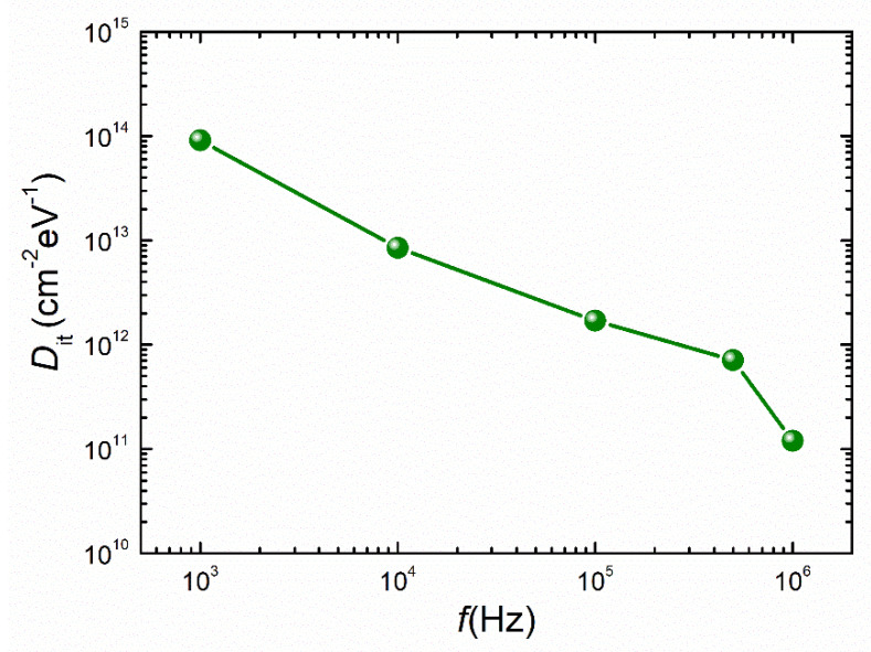
We used capacitance-voltage (-), conductance-voltage (-), and noise measurements to examine the carrier trap mechanisms at the surface/core of an AlGaN/GaN nanowire wrap-gate transistor (WGT). When the frequency is increased, the predicted surface trap density promptly drops, with values ranging from 9.1 × 10 eV∙cm at 1 kHz to 1.2 × 10 eV∙cm at 1 MHz. The power spectral density exhibits 1/-noise behavior in the barrier accumulation area and rises with gate bias, according to the 1/-noise features. At lower frequencies, the device exhibits 1/-noise behavior, while beyond 1 kHz, it exhibits 1/-noise behavior. Additionally, when the fabricated device governs in the deep-subthreshold regime, the cutoff frequency for the 1/-noise features moves to the subordinated frequency (~10 Hz) side.

摘要

我们使用电容 - 电压(-)、电导 - 电压(-)和噪声测量来研究AlGaN/GaN纳米线环绕栅晶体管(WGT)表面/核心处的载流子陷阱机制。当频率增加时,预测的表面陷阱密度迅速下降,其值范围从1 kHz时的9.1×10 eV∙cm到1 MHz时的1.2×10 eV∙cm。根据1/-噪声特征,功率谱密度在势垒积累区域呈现1/-噪声行为,并随栅极偏置而上升。在较低频率下,该器件呈现1/-噪声行为,而在超过1 kHz时,它呈现1/-噪声行为。此外,当制造的器件在深亚阈值区域工作时,1/-噪声特征的截止频率移向从属频率(~10 Hz)一侧。

https://cdn.ncbi.nlm.nih.gov/pmc/blobs/2443/10386025/c6048ea36c02/nanomaterials-13-02132-g005.jpg
https://cdn.ncbi.nlm.nih.gov/pmc/blobs/2443/10386025/a68cea37c052/nanomaterials-13-02132-g001.jpg
https://cdn.ncbi.nlm.nih.gov/pmc/blobs/2443/10386025/926b33c9a949/nanomaterials-13-02132-g002.jpg
https://cdn.ncbi.nlm.nih.gov/pmc/blobs/2443/10386025/17d518e092da/nanomaterials-13-02132-g003.jpg
https://cdn.ncbi.nlm.nih.gov/pmc/blobs/2443/10386025/3803e5f8f763/nanomaterials-13-02132-g004.jpg
https://cdn.ncbi.nlm.nih.gov/pmc/blobs/2443/10386025/c6048ea36c02/nanomaterials-13-02132-g005.jpg

相似文献

1
Carrier Trap and Their Effects on the Surface and Core of AlGaN/GaN Nanowire Wrap-Gate Transistor.载流子陷阱及其对氮化铝镓/氮化镓纳米线环绕栅晶体管表面和核心的影响。
Nanomaterials (Basel). 2023 Jul 22;13(14):2132. doi: 10.3390/nano13142132.
2
Graphene as a Schottky Barrier Contact to AlGaN/GaN Heterostructures.石墨烯作为AlGaN/GaN异质结构的肖特基势垒接触
Materials (Basel). 2020 Sep 17;13(18):4140. doi: 10.3390/ma13184140.
3
Temperature-Dependent Carrier Transport in GaN Nanowire Wrap-Gate Transistor.氮化镓纳米线环绕栅晶体管中与温度相关的载流子输运
Nanomaterials (Basel). 2023 May 12;13(10):1629. doi: 10.3390/nano13101629.
4
Barrier Height, Ideality Factor and Role of Inhomogeneities at the AlGaN/GaN Interface in GaN Nanowire Wrap-Gate Transistor.氮化镓纳米线环绕栅晶体管中AlGaN/GaN界面的势垒高度、理想因子及不均匀性的作用
Nanomaterials (Basel). 2023 Dec 17;13(24):3159. doi: 10.3390/nano13243159.
5
Double-Quantum-Well AlGaN/GaN Field Effect Transistors with Top and Back Gates: Electrical and Noise Characteristics.具有顶栅和背栅的双量子阱AlGaN/GaN场效应晶体管:电学和噪声特性
Micromachines (Basel). 2021 Jun 19;12(6):721. doi: 10.3390/mi12060721.
6
Characteristics of GaN-Based Nanowire Gate-All-Around (GAA) Transistors.基于氮化镓的全环绕纳米线(GAA)晶体管的特性
J Nanosci Nanotechnol. 2020 Jul 1;20(7):4282-4286. doi: 10.1166/jnn.2020.17784.
7
AlGaN/GaN on SiC Devices without a GaN Buffer Layer: Electrical and Noise Characteristics.碳化硅衬底上无氮化镓缓冲层的氮化铝镓/氮化镓器件:电学和噪声特性
Micromachines (Basel). 2020 Dec 20;11(12):1131. doi: 10.3390/mi11121131.
8
A mixer architecture using GaN-based split-gate nanowire transistor.
Nanotechnology. 2024 Jul 24;35(41). doi: 10.1088/1361-6528/ad63b0.
9
A quantitative approach for trap analysis between AlGaN and GaN in high electron mobility transistors.一种用于分析高电子迁移率晶体管中 AlGaN 与 GaN 之间势垒的定量方法。
Sci Rep. 2021 Nov 17;11(1):22401. doi: 10.1038/s41598-021-01768-4.
10
Charging Effect by Fluorine-Treatment and Recess Gate for Enhancement-Mode on AlGaN/GaN High Electron Mobility Transistors.通过氟处理和凹槽栅极对AlGaN/GaN高电子迁移率晶体管增强模式的充电效应。
Nanomaterials (Basel). 2020 Oct 24;10(11):2116. doi: 10.3390/nano10112116.

引用本文的文献

1
Effects of Carrier Trapping and Noise in Triangular-Shaped GaN Nanowire Wrap-Gate Transistor.三角形氮化镓纳米线环绕栅晶体管中载流子俘获和噪声的影响
Nanomaterials (Basel). 2025 Aug 30;15(17):1336. doi: 10.3390/nano15171336.
2
Barrier Height, Ideality Factor and Role of Inhomogeneities at the AlGaN/GaN Interface in GaN Nanowire Wrap-Gate Transistor.氮化镓纳米线环绕栅晶体管中AlGaN/GaN界面的势垒高度、理想因子及不均匀性的作用
Nanomaterials (Basel). 2023 Dec 17;13(24):3159. doi: 10.3390/nano13243159.

本文引用的文献

1
Temperature-Dependent Carrier Transport in GaN Nanowire Wrap-Gate Transistor.氮化镓纳米线环绕栅晶体管中与温度相关的载流子输运
Nanomaterials (Basel). 2023 May 12;13(10):1629. doi: 10.3390/nano13101629.
2
Semiconductor nanowire: what's next?半导体纳米线:下一步是什么?
Nano Lett. 2010 May 12;10(5):1529-36. doi: 10.1021/nl100665r.
3
Investigation on localized states in GaN nanowires.氮化镓纳米线中局域态的研究。
ACS Nano. 2008 Feb;2(2):287-92. doi: 10.1021/nn700386w.