• 文献检索
  • 文档翻译
  • 深度研究
  • 学术资讯
  • Suppr Zotero 插件Zotero 插件
  • 邀请有礼
  • 套餐&价格
  • 历史记录
应用&插件
Suppr Zotero 插件Zotero 插件浏览器插件Mac 客户端Windows 客户端微信小程序
定价
高级版会员购买积分包购买API积分包
服务
文献检索文档翻译深度研究API 文档MCP 服务
关于我们
关于 Suppr公司介绍联系我们用户协议隐私条款
关注我们

Suppr 超能文献

核心技术专利:CN118964589B侵权必究
粤ICP备2023148730 号-1Suppr @ 2026

文献检索

告别复杂PubMed语法,用中文像聊天一样搜索,搜遍4000万医学文献。AI智能推荐,让科研检索更轻松。

立即免费搜索

文件翻译

保留排版,准确专业,支持PDF/Word/PPT等文件格式,支持 12+语言互译。

免费翻译文档

深度研究

AI帮你快速写综述,25分钟生成高质量综述,智能提取关键信息,辅助科研写作。

立即免费体验

采用具有锗源和电荷增强绝缘的外延隧道层的电感式线隧穿场效应晶体管。

Inductive line tunneling FET using epitaxial tunnel layer with Ge-source and charge enhancement insulation.

作者信息

Lin Jyi-Tsong, Chang Yen-Chen

机构信息

Department of Electrical Engineering, National Sun Yat-Sen University, Kaohsiung, 80424, Taiwan, ROC.

出版信息

Discov Nano. 2023 Aug 5;18(1):99. doi: 10.1186/s11671-023-03878-6.

DOI:10.1186/s11671-023-03878-6
PMID:37542560
原文链接:https://pmc.ncbi.nlm.nih.gov/articles/PMC10404213/
Abstract

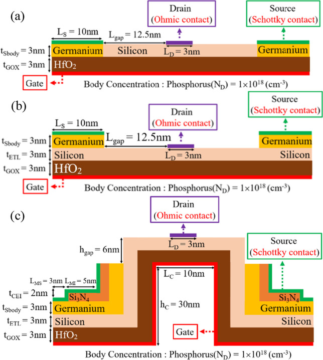
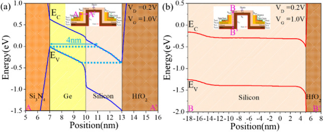
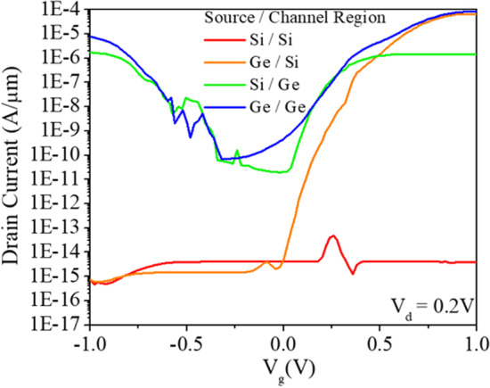
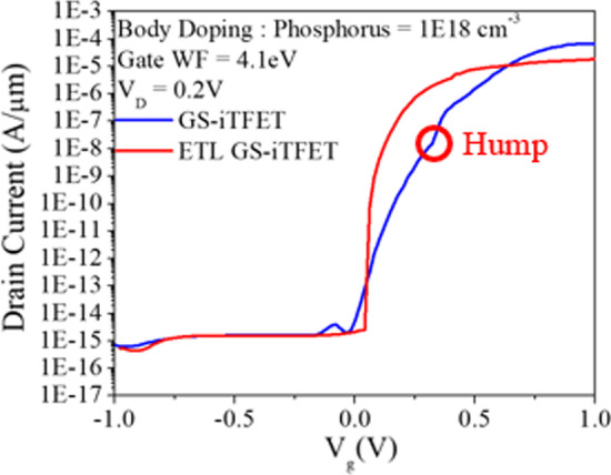
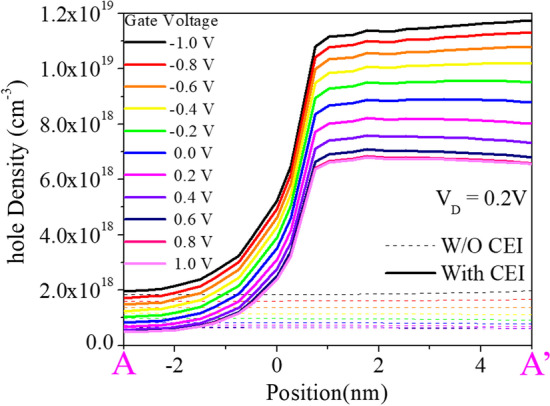
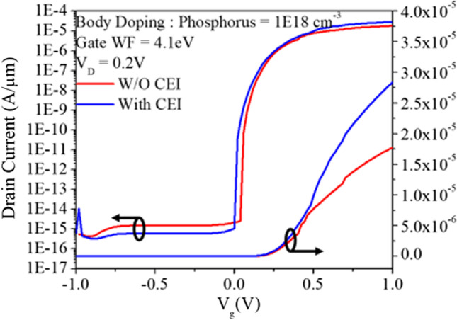
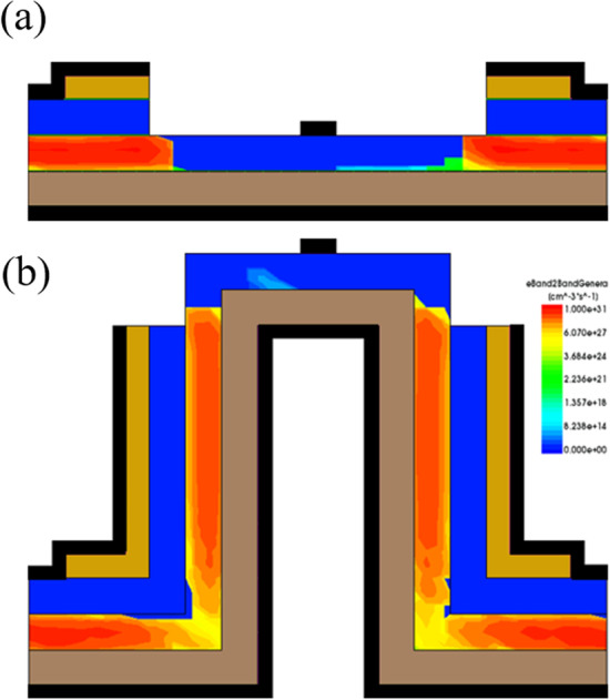
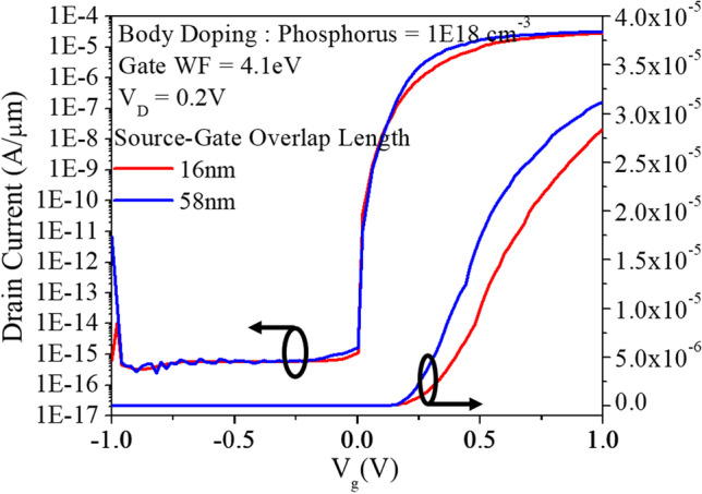
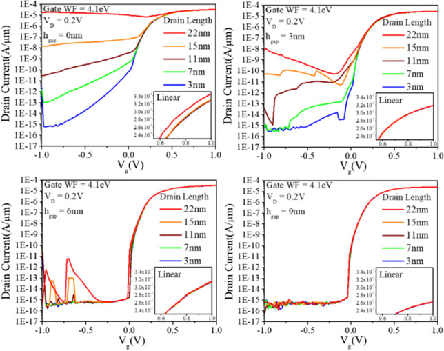
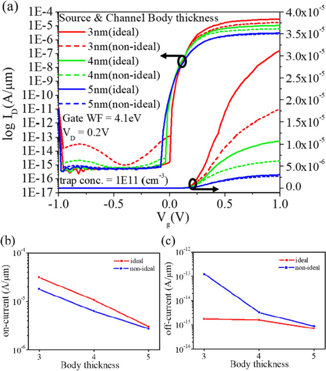
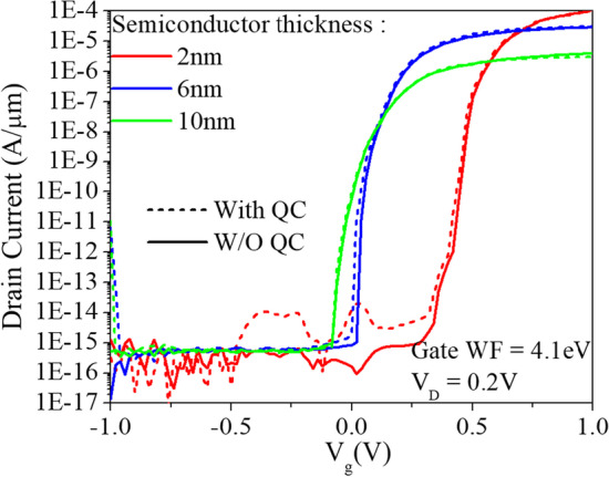
In this paper, we propose an inductive line tunneling FET using Epitaxial Tunnel Layer with Ge-Source and Charge Enhancement Insulation (CEI ETL GS-iTFET). The CEI ETL GS-iTFET allows full overlap between the gate and source regions, thereby enhancing the line tunneling. In addition, a germanium layer is introduced on the source side to form a heterojunction, effectively improving the device's conduction current. An ETL is incorporated to combat point tunneling leakage, resulting in a steeper subthreshold swing. Furthermore, a CEI consisting of SiN is introduced between the germanium source and the Schottky metal, which effectively reduces carrier losses in the inversion layer and improves the overall device performance. This study presents a calibration-based approach to simulations, taking into account practical process considerations. Simulation results show that at V = 0.2 V, the CEI ETL GS-iTFET achieves an average subthreshold swing (SS) of 30.5 mV/dec, an I of 3.12 × 10 A/μm and an I/I ratio of 1.81 × 10. These results demonstrate a significantly low subthreshold swing and a high current ratio of about 10. In addition, the proposed device eliminates the need for multiple implantation processes, resulting in significant manufacturing cost reductions. As a result, the CEI ETL GS-iTFET shows remarkable potential in future low-power device competition.

摘要

在本文中,我们提出了一种采用具有锗源和电荷增强绝缘(CEI ETL GS-iTFET)的外延隧道层的电感式线隧穿场效应晶体管。CEI ETL GS-iTFET允许栅极和源极区域完全重叠,从而增强线隧穿。此外,在源极侧引入锗层以形成异质结,有效提高了器件的传导电流。并入一个ETL以对抗点隧穿泄漏,从而获得更陡的亚阈值摆幅。此外,在锗源极和肖特基金属之间引入了由SiN组成的CEI,这有效地减少了反型层中的载流子损耗并提高了整体器件性能。本研究提出了一种基于校准的模拟方法,同时考虑了实际工艺因素。模拟结果表明,在V = 0.2 V时,CEI ETL GS-iTFET的平均亚阈值摆幅(SS)为30.5 mV/dec,I为3.12×10 A/μm,I/I比为1.81×10。这些结果表明亚阈值摆幅极低且电流比约为10。此外,所提出的器件无需多次注入工艺,从而显著降低了制造成本。因此,CEI ETL GS-iTFET在未来低功耗器件竞争中显示出显著的潜力。

https://cdn.ncbi.nlm.nih.gov/pmc/blobs/d6e1/10404213/83563ef08549/11671_2023_3878_Fig21_HTML.jpg
https://cdn.ncbi.nlm.nih.gov/pmc/blobs/d6e1/10404213/5a9795c36e5d/11671_2023_3878_Fig1_HTML.jpg
https://cdn.ncbi.nlm.nih.gov/pmc/blobs/d6e1/10404213/fd5679da7092/11671_2023_3878_Fig2_HTML.jpg
https://cdn.ncbi.nlm.nih.gov/pmc/blobs/d6e1/10404213/26f42279b600/11671_2023_3878_Fig3_HTML.jpg
https://cdn.ncbi.nlm.nih.gov/pmc/blobs/d6e1/10404213/cba95c865498/11671_2023_3878_Fig4_HTML.jpg
https://cdn.ncbi.nlm.nih.gov/pmc/blobs/d6e1/10404213/ac721bc37a0b/11671_2023_3878_Fig5_HTML.jpg
https://cdn.ncbi.nlm.nih.gov/pmc/blobs/d6e1/10404213/642c15a2f3a8/11671_2023_3878_Fig6_HTML.jpg
https://cdn.ncbi.nlm.nih.gov/pmc/blobs/d6e1/10404213/94fc41287d40/11671_2023_3878_Fig7_HTML.jpg
https://cdn.ncbi.nlm.nih.gov/pmc/blobs/d6e1/10404213/09fd568ef604/11671_2023_3878_Fig8_HTML.jpg
https://cdn.ncbi.nlm.nih.gov/pmc/blobs/d6e1/10404213/f0bc511c0b71/11671_2023_3878_Fig9_HTML.jpg
https://cdn.ncbi.nlm.nih.gov/pmc/blobs/d6e1/10404213/d41f2a7271da/11671_2023_3878_Fig10_HTML.jpg
https://cdn.ncbi.nlm.nih.gov/pmc/blobs/d6e1/10404213/b61af38e98a8/11671_2023_3878_Fig11_HTML.jpg
https://cdn.ncbi.nlm.nih.gov/pmc/blobs/d6e1/10404213/9bdf6de69195/11671_2023_3878_Fig12_HTML.jpg
https://cdn.ncbi.nlm.nih.gov/pmc/blobs/d6e1/10404213/828236449a6a/11671_2023_3878_Fig13_HTML.jpg
https://cdn.ncbi.nlm.nih.gov/pmc/blobs/d6e1/10404213/cc7422d1d28c/11671_2023_3878_Fig14_HTML.jpg
https://cdn.ncbi.nlm.nih.gov/pmc/blobs/d6e1/10404213/f3788a386911/11671_2023_3878_Fig15_HTML.jpg
https://cdn.ncbi.nlm.nih.gov/pmc/blobs/d6e1/10404213/5e735392beb3/11671_2023_3878_Fig16_HTML.jpg
https://cdn.ncbi.nlm.nih.gov/pmc/blobs/d6e1/10404213/31dd2d6f69f4/11671_2023_3878_Fig17_HTML.jpg
https://cdn.ncbi.nlm.nih.gov/pmc/blobs/d6e1/10404213/289affed4990/11671_2023_3878_Fig18_HTML.jpg
https://cdn.ncbi.nlm.nih.gov/pmc/blobs/d6e1/10404213/e6205a7a3243/11671_2023_3878_Fig19_HTML.jpg
https://cdn.ncbi.nlm.nih.gov/pmc/blobs/d6e1/10404213/6a94c376e5fb/11671_2023_3878_Fig20_HTML.jpg
https://cdn.ncbi.nlm.nih.gov/pmc/blobs/d6e1/10404213/83563ef08549/11671_2023_3878_Fig21_HTML.jpg

相似文献

1
Inductive line tunneling FET using epitaxial tunnel layer with Ge-source and charge enhancement insulation.采用具有锗源和电荷增强绝缘的外延隧道层的电感式线隧穿场效应晶体管。
Discov Nano. 2023 Aug 5;18(1):99. doi: 10.1186/s11671-023-03878-6.
2
FS-iTFET: advancing tunnel FET technology with Schottky-inductive source and GAA design.FS-iTFET:采用肖特基电感源和全栅极架构推进隧道场效应晶体管技术
Discov Nano. 2024 Sep 4;19(1):140. doi: 10.1186/s11671-024-04096-4.
3
Enhancing subthreshold slope and ON-current in a simple iTFET with overlapping gate on source-contact, drain Schottky contact, and intrinsic SiGe-pocket.在具有源极接触上重叠栅极、漏极肖特基接触和本征硅锗口袋的简单交错隧穿场效应晶体管中提高亚阈值斜率和导通电流。
Discov Nano. 2023 Sep 29;18(1):121. doi: 10.1186/s11671-023-03904-7.
4
A new line tunneling SiGe/Si iTFET with control gate for leakage suppression and subthreshold swing improvement.一种具有控制栅极的新型线隧穿硅锗/硅绝缘栅场效应晶体管,用于抑制漏电流和改善亚阈值摆幅。
Discov Nano. 2023 Jul 28;18(1):96. doi: 10.1186/s11671-023-03875-9.
5
Investigation of SiGe/Si heterojunction inductive line tunneling TFET with source Schottky contact for prospect ultra-low power applications.用于前景广阔的超低功耗应用的具有源极肖特基接触的SiGe/Si异质结电感式线隧穿场效应晶体管的研究。
Nanotechnology. 2024 Jan 30;35(16). doi: 10.1088/1361-6528/ad1d7a.
6
Nanosheet integration of induced tunnel field-effect transistor with lower cost and lower power.具有更低成本和更低功耗的诱导隧道场效应晶体管的纳米片集成。
Discov Nano. 2024 Jul 2;19(1):108. doi: 10.1186/s11671-024-04036-2.
7
Analog/RF Performance of T-Shape Gate Dual-Source Tunnel Field-Effect Transistor.T 形栅极双源极隧道场效应晶体管的模拟/射频性能
Nanoscale Res Lett. 2018 Oct 12;13(1):321. doi: 10.1186/s11671-018-2723-y.
8
Bilateral sidewall engineering SiGeiTFET for low power display application.用于低功耗显示应用的双边侧壁工程硅锗鳍式场效应晶体管
Nanotechnology. 2023 Oct 4;34(50). doi: 10.1088/1361-6528/acf9ab.
9
The role of the Ge mole fraction in improving the performance of a nanoscale junctionless tunneling FET: concept and scaling capability.锗摩尔分数在提高纳米级无结隧穿场效应晶体管性能中的作用:概念与缩放能力。
Beilstein J Nanotechnol. 2018 Jun 22;9:1856-1862. doi: 10.3762/bjnano.9.177. eCollection 2018.
10
Design and Optimization of Germanium-Based Gate-Metal-Core Vertical Nanowire Tunnel FET.锗基栅极-金属芯垂直纳米线隧道场效应晶体管的设计与优化
Micromachines (Basel). 2019 Oct 31;10(11):749. doi: 10.3390/mi10110749.

引用本文的文献

1
A novel ultra-steep subthreshold swing iTFET with control gate and control source biasing.一种具有控制栅极和控制源极偏置的新型超陡亚阈值摆幅绝缘栅场效应晶体管。
Sci Rep. 2025 Aug 2;15(1):28207. doi: 10.1038/s41598-025-13011-5.