• 文献检索
  • 文档翻译
  • 深度研究
  • 学术资讯
  • Suppr Zotero 插件Zotero 插件
  • 邀请有礼
  • 套餐&价格
  • 历史记录
应用&插件
Suppr Zotero 插件Zotero 插件浏览器插件Mac 客户端Windows 客户端微信小程序
定价
高级版会员购买积分包购买API积分包
服务
文献检索文档翻译深度研究API 文档MCP 服务
关于我们
关于 Suppr公司介绍联系我们用户协议隐私条款
关注我们

Suppr 超能文献

核心技术专利:CN118964589B侵权必究
粤ICP备2023148730 号-1Suppr @ 2026

文献检索

告别复杂PubMed语法,用中文像聊天一样搜索,搜遍4000万医学文献。AI智能推荐,让科研检索更轻松。

立即免费搜索

文件翻译

保留排版,准确专业,支持PDF/Word/PPT等文件格式,支持 12+语言互译。

免费翻译文档

深度研究

AI帮你快速写综述,25分钟生成高质量综述,智能提取关键信息,辅助科研写作。

立即免费体验

FS-iTFET:采用肖特基电感源和全栅极架构推进隧道场效应晶体管技术

FS-iTFET: advancing tunnel FET technology with Schottky-inductive source and GAA design.

作者信息

Lin Jyi-Tsong, Tai Wei-Heng

机构信息

Department of Electrical Engineering, National Sun Yat-Sen University, Kaohsiung, 80424, Taiwan, ROC.

出版信息

Discov Nano. 2024 Sep 4;19(1):140. doi: 10.1186/s11671-024-04096-4.

DOI:10.1186/s11671-024-04096-4
PMID:39227488
原文链接:https://pmc.ncbi.nlm.nih.gov/articles/PMC11371965/
Abstract

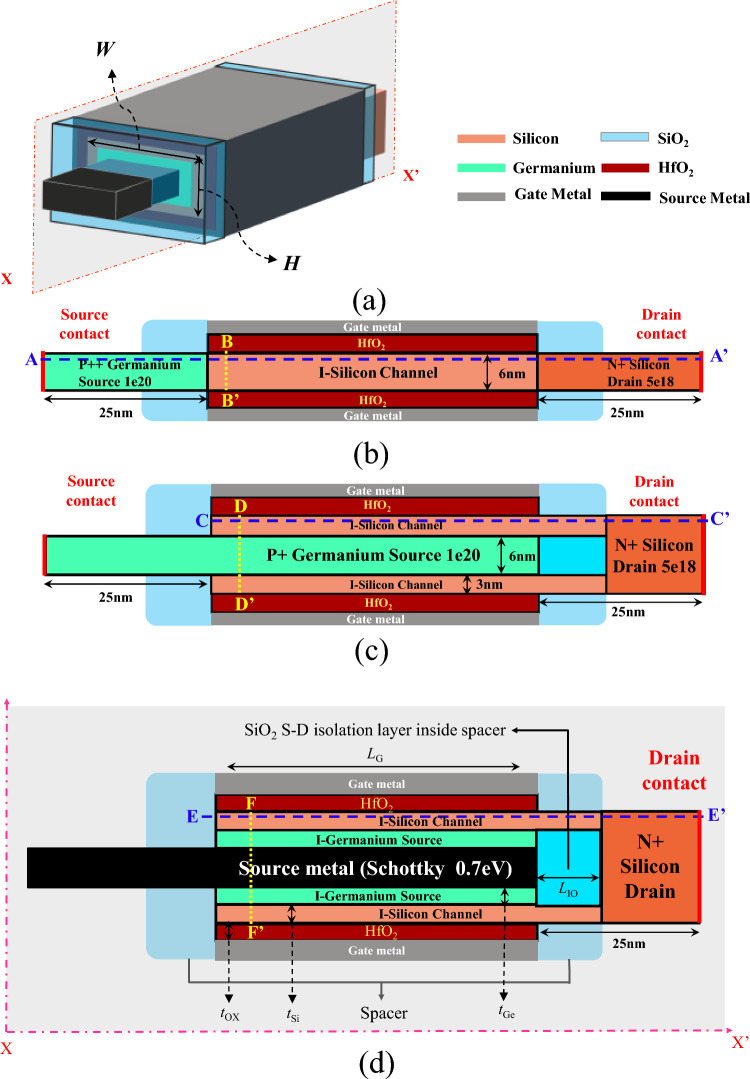
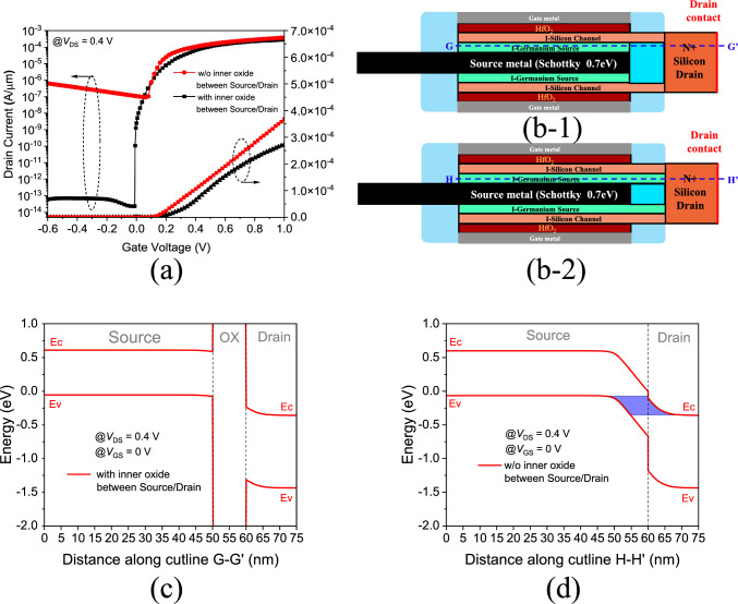
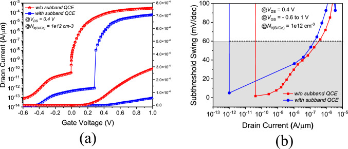
In this paper, we introduce a novel Forkshape nanosheet Inductive Tunnel Field-Effect Transistor (FS-iTFET) featuring a Gate-All-Around structure and a full-line tunneling heterojunction channel. The overlapping gate and source contact regions create a strong and uniform electric field in the channel. Furthermore, the metal-semiconductor Schottky junction in the intrinsic source region induces the required carriers without the need for doping. This innovative design achieves both a steeper subthreshold swing (SS) and a higher ON-state current (I). Using calibration-based simulations with Sentaurus TCAD, we compare the performance of three newly designed device structures: the conventional Nanosheet Tunnel Field-Effect Transistor (NS-TFET), the Nanosheet Line-tunneling TFET (NS-LTFET), and the proposed FS-iTFET. Simulation results show that, compared to the traditional NS-TFET, the NS-LTFET with its full line-tunneling structure improves the average subthreshold swing (SS) by 19.2%. More significantly, the FS-iTFET, utilizing the Schottky-inductive source, further improves the SS by 49% and achieves a superior I/I ratio. Additionally, we explore the impact of Trap-Assisted Tunneling on the performance of the three different integrations. The FS-iTFET consistently demonstrates superior performance across various metrics, highlighting its potential in advancing tunnel field-effect transistor technology.

摘要

在本文中,我们介绍了一种新型的叉形纳米片感应隧道场效应晶体管(FS-iTFET),它具有全方位栅极结构和全线隧穿异质结沟道。重叠的栅极和源极接触区域在沟道中产生了强大且均匀的电场。此外,本征源区中的金属 - 半导体肖特基结无需掺杂即可诱导出所需的载流子。这种创新设计实现了更陡的亚阈值摆幅(SS)和更高的导通态电流(I)。使用Sentaurus TCAD基于校准的模拟,我们比较了三种新设计的器件结构的性能:传统的纳米片隧道场效应晶体管(NS-TFET)、纳米片线隧穿TFET(NS-LTFET)和所提出的FS-iTFET。模拟结果表明,与传统的NS-TFET相比,具有全线隧穿结构的NS-LTFET将平均亚阈值摆幅(SS)提高了19.2%。更显著的是,利用肖特基感应源的FS-iTFET进一步将SS提高了49%,并实现了优异的I/I比。此外,我们探讨了陷阱辅助隧穿对三种不同集成性能的影响。FS-iTFET在各项指标上始终表现出卓越的性能,突出了其在推进隧道场效应晶体管技术方面的潜力。

https://cdn.ncbi.nlm.nih.gov/pmc/blobs/c054/11371965/c512377805e2/11671_2024_4096_Fig16_HTML.jpg
https://cdn.ncbi.nlm.nih.gov/pmc/blobs/c054/11371965/3ed72764a63b/11671_2024_4096_Fig1_HTML.jpg
https://cdn.ncbi.nlm.nih.gov/pmc/blobs/c054/11371965/ab1abce8df2e/11671_2024_4096_Fig2_HTML.jpg
https://cdn.ncbi.nlm.nih.gov/pmc/blobs/c054/11371965/7ce6c8561deb/11671_2024_4096_Fig3_HTML.jpg
https://cdn.ncbi.nlm.nih.gov/pmc/blobs/c054/11371965/5c050830755b/11671_2024_4096_Fig5_HTML.jpg
https://cdn.ncbi.nlm.nih.gov/pmc/blobs/c054/11371965/24fbfe0d5527/11671_2024_4096_Fig6_HTML.jpg
https://cdn.ncbi.nlm.nih.gov/pmc/blobs/c054/11371965/ef06d5a834f0/11671_2024_4096_Fig9_HTML.jpg
https://cdn.ncbi.nlm.nih.gov/pmc/blobs/c054/11371965/0c164214a726/11671_2024_4096_Fig10_HTML.jpg
https://cdn.ncbi.nlm.nih.gov/pmc/blobs/c054/11371965/933bea717bbf/11671_2024_4096_Fig11_HTML.jpg
https://cdn.ncbi.nlm.nih.gov/pmc/blobs/c054/11371965/94420e1f418e/11671_2024_4096_Fig12_HTML.jpg
https://cdn.ncbi.nlm.nih.gov/pmc/blobs/c054/11371965/dfe4297a8128/11671_2024_4096_Fig13_HTML.jpg
https://cdn.ncbi.nlm.nih.gov/pmc/blobs/c054/11371965/84bc30987523/11671_2024_4096_Fig14_HTML.jpg
https://cdn.ncbi.nlm.nih.gov/pmc/blobs/c054/11371965/e90937f2d6c2/11671_2024_4096_Fig15_HTML.jpg
https://cdn.ncbi.nlm.nih.gov/pmc/blobs/c054/11371965/c512377805e2/11671_2024_4096_Fig16_HTML.jpg

相似文献

1
FS-iTFET: advancing tunnel FET technology with Schottky-inductive source and GAA design.FS-iTFET:采用肖特基电感源和全栅极架构推进隧道场效应晶体管技术
Discov Nano. 2024 Sep 4;19(1):140. doi: 10.1186/s11671-024-04096-4.
2
Nanosheet integration of induced tunnel field-effect transistor with lower cost and lower power.具有更低成本和更低功耗的诱导隧道场效应晶体管的纳米片集成。
Discov Nano. 2024 Jul 2;19(1):108. doi: 10.1186/s11671-024-04036-2.
3
Inductive line tunneling FET using epitaxial tunnel layer with Ge-source and charge enhancement insulation.采用具有锗源和电荷增强绝缘的外延隧道层的电感式线隧穿场效应晶体管。
Discov Nano. 2023 Aug 5;18(1):99. doi: 10.1186/s11671-023-03878-6.
4
Enhancing subthreshold slope and ON-current in a simple iTFET with overlapping gate on source-contact, drain Schottky contact, and intrinsic SiGe-pocket.在具有源极接触上重叠栅极、漏极肖特基接触和本征硅锗口袋的简单交错隧穿场效应晶体管中提高亚阈值斜率和导通电流。
Discov Nano. 2023 Sep 29;18(1):121. doi: 10.1186/s11671-023-03904-7.
5
Investigation of SiGe/Si heterojunction inductive line tunneling TFET with source Schottky contact for prospect ultra-low power applications.用于前景广阔的超低功耗应用的具有源极肖特基接触的SiGe/Si异质结电感式线隧穿场效应晶体管的研究。
Nanotechnology. 2024 Jan 30;35(16). doi: 10.1088/1361-6528/ad1d7a.
6
A new line tunneling SiGe/Si iTFET with control gate for leakage suppression and subthreshold swing improvement.一种具有控制栅极的新型线隧穿硅锗/硅绝缘栅场效应晶体管,用于抑制漏电流和改善亚阈值摆幅。
Discov Nano. 2023 Jul 28;18(1):96. doi: 10.1186/s11671-023-03875-9.
7
A Novel Germanium-Around-Source Gate-All-Around tunnelling Field-Effect Transistor for Low-Power Applications.一种用于低功耗应用的新型源极周围锗栅全环绕隧道场效应晶体管。
Micromachines (Basel). 2020 Feb 3;11(2):164. doi: 10.3390/mi11020164.
8
Analog/RF Performance of T-Shape Gate Dual-Source Tunnel Field-Effect Transistor.T 形栅极双源极隧道场效应晶体管的模拟/射频性能
Nanoscale Res Lett. 2018 Oct 12;13(1):321. doi: 10.1186/s11671-018-2723-y.
9
Polarization Gradient Effect of Negative Capacitance LTFET.负电容横向隧穿场效应晶体管的极化梯度效应
Micromachines (Basel). 2022 Feb 22;13(3):344. doi: 10.3390/mi13030344.
10
Design Optimization of Ge/GaAs-Based Heterojunction Gate-All-Around (GAA) Arch-Shaped Tunneling Field-Effect Transistor (A-TFET).基于Ge/GaAs的异质结全栅环绕(GAA)拱形隧道场效应晶体管(A-TFET)的设计优化
J Nanosci Nanotechnol. 2018 Sep 1;18(9):6602-6605. doi: 10.1166/jnn.2018.15705.

本文引用的文献

1
Enhancing subthreshold slope and ON-current in a simple iTFET with overlapping gate on source-contact, drain Schottky contact, and intrinsic SiGe-pocket.在具有源极接触上重叠栅极、漏极肖特基接触和本征硅锗口袋的简单交错隧穿场效应晶体管中提高亚阈值斜率和导通电流。
Discov Nano. 2023 Sep 29;18(1):121. doi: 10.1186/s11671-023-03904-7.
2
DC and AC characteristics of Si/SiGe based vertically stacked complementary-tunneling FETs.基于硅/锗硅的垂直堆叠互补隧穿场效应晶体管的直流和交流特性
Nanotechnology. 2023 Oct 11;34(50). doi: 10.1088/1361-6528/acfb11.
3
Study of Silicon Nitride Inner Spacer Formation in Process of Gate-all-around Nano-Transistors.
环绕栅纳米晶体管工艺中氮化硅内间隔层形成的研究
Nanomaterials (Basel). 2020 Apr 20;10(4):793. doi: 10.3390/nano10040793.
4
Selective Wet Etching of Silicon Germanium in Composite Vertical Nanowires.复合垂直纳米线中硅锗的选择性湿法刻蚀。
ACS Appl Mater Interfaces. 2019 Oct 9;11(40):36839-36846. doi: 10.1021/acsami.9b11934. Epub 2019 Sep 26.
5
Tunnel field-effect transistors as energy-efficient electronic switches.隧道场效应晶体管作为节能电子开关。
Nature. 2011 Nov 16;479(7373):329-37. doi: 10.1038/nature10679.
6
Nanowire transistors without junctions.无结纳米线晶体管。
Nat Nanotechnol. 2010 Mar;5(3):225-9. doi: 10.1038/nnano.2010.15. Epub 2010 Feb 21.