• 文献检索
  • 文档翻译
  • 深度研究
  • 学术资讯
  • Suppr Zotero 插件Zotero 插件
  • 邀请有礼
  • 套餐&价格
  • 历史记录
应用&插件
Suppr Zotero 插件Zotero 插件浏览器插件Mac 客户端Windows 客户端微信小程序
定价
高级版会员购买积分包购买API积分包
服务
文献检索文档翻译深度研究API 文档MCP 服务
关于我们
关于 Suppr公司介绍联系我们用户协议隐私条款
关注我们

Suppr 超能文献

核心技术专利:CN118964589B侵权必究
粤ICP备2023148730 号-1Suppr @ 2026

文献检索

告别复杂PubMed语法,用中文像聊天一样搜索,搜遍4000万医学文献。AI智能推荐,让科研检索更轻松。

立即免费搜索

文件翻译

保留排版,准确专业,支持PDF/Word/PPT等文件格式,支持 12+语言互译。

免费翻译文档

深度研究

AI帮你快速写综述,25分钟生成高质量综述,智能提取关键信息,辅助科研写作。

立即免费体验

通过金属辅助化学蚀刻结合微振动制备硅纳米线

Fabrication of Silicon Nanowires by Metal-Assisted Chemical Etching Combined with Micro-Vibration.

作者信息

Huang Weiye, Wu Junyi, Li Wenxin, Chen Guojin, Chu Changyong, Li Chao, Zhu Yucheng, Yang Hui, Chao Yan

机构信息

School of Mechanical Engineering, Hangzhou Dianzi University, Hangzhou 310018, China.

Sanmen Sanyou Technology Inc., Taizhou 472000, China.

出版信息

Materials (Basel). 2023 Aug 5;16(15):5483. doi: 10.3390/ma16155483.

DOI:10.3390/ma16155483
PMID:37570187
原文链接:https://pmc.ncbi.nlm.nih.gov/articles/PMC10420322/
Abstract

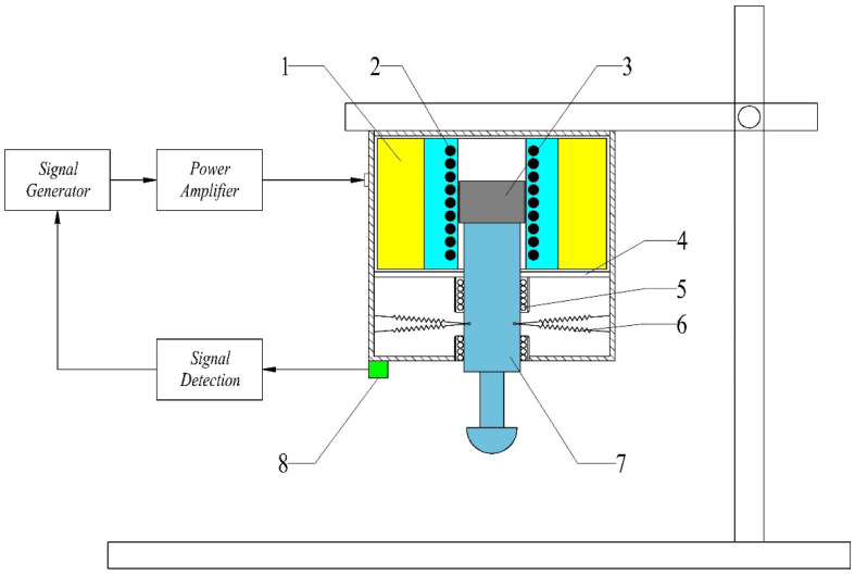
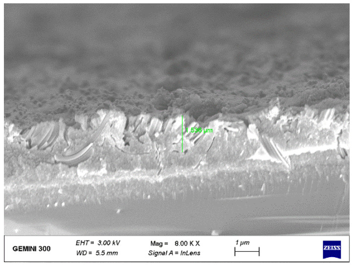
In this work, we design a micro-vibration platform, which combined with the traditional metal-assisted chemical etching (MaCE) to etch silicon nanowires (SiNWs). The etching mechanism of SiNWs, including in the mass-transport (MT) and charge-transport (CT) processes, was explored through the characterization of SiNW's length as a function of MaCE combined with micro-vibration conditions, such as vibration amplitude and frequency. The scanning electron microscope (SEM) experimental results indicated that the etching rate would be continuously improved with an increase in amplitude and reached its maximum at 4 μm. Further increasing amplitude reduced the etching rate and affected the morphology of the SiNWs. Adjusting the vibration frequency would result in a maximum etching rate at a frequency of 20 Hz, and increasing the frequency will not help to improve the etching effects.

摘要

在这项工作中,我们设计了一个微振动平台,该平台与传统的金属辅助化学蚀刻(MaCE)相结合来蚀刻硅纳米线(SiNWs)。通过将SiNW的长度表征为MaCE与微振动条件(如振动幅度和频率)的函数,探索了SiNWs的蚀刻机制,包括质量传输(MT)和电荷传输(CT)过程。扫描电子显微镜(SEM)实验结果表明,蚀刻速率会随着振幅的增加而持续提高,并在4μm时达到最大值。进一步增加振幅会降低蚀刻速率并影响SiNWs的形态。调整振动频率会在20Hz的频率下产生最大蚀刻速率,而增加频率无助于提高蚀刻效果。

https://cdn.ncbi.nlm.nih.gov/pmc/blobs/d23c/10420322/fc748754f2ca/materials-16-05483-g007.jpg
https://cdn.ncbi.nlm.nih.gov/pmc/blobs/d23c/10420322/312b47f7ac38/materials-16-05483-g001.jpg
https://cdn.ncbi.nlm.nih.gov/pmc/blobs/d23c/10420322/5c7d4fb72a97/materials-16-05483-g002.jpg
https://cdn.ncbi.nlm.nih.gov/pmc/blobs/d23c/10420322/bc512a6577b5/materials-16-05483-g003.jpg
https://cdn.ncbi.nlm.nih.gov/pmc/blobs/d23c/10420322/65fe4360c83c/materials-16-05483-g004.jpg
https://cdn.ncbi.nlm.nih.gov/pmc/blobs/d23c/10420322/37126fe437a4/materials-16-05483-g005.jpg
https://cdn.ncbi.nlm.nih.gov/pmc/blobs/d23c/10420322/4e57fb276e9c/materials-16-05483-g006.jpg
https://cdn.ncbi.nlm.nih.gov/pmc/blobs/d23c/10420322/fc748754f2ca/materials-16-05483-g007.jpg

相似文献

1
Fabrication of Silicon Nanowires by Metal-Assisted Chemical Etching Combined with Micro-Vibration.通过金属辅助化学蚀刻结合微振动制备硅纳米线
Materials (Basel). 2023 Aug 5;16(15):5483. doi: 10.3390/ma16155483.
2
Unraveling the Morphological Evolution and Etching Kinetics of Porous Silicon Nanowires During Metal-Assisted Chemical Etching.揭示金属辅助化学蚀刻过程中多孔硅纳米线的形态演变和蚀刻动力学
Nanoscale Res Lett. 2017 Dec;12(1):385. doi: 10.1186/s11671-017-2156-z. Epub 2017 Jun 2.
3
Enhanced photocatalytic activities of silicon nanowires/graphene oxide nanocomposite: Effect of etching parameters.硅纳米线/氧化石墨烯纳米复合材料光催化活性的增强:刻蚀参数的影响。
J Environ Sci (China). 2021 Mar;101:123-134. doi: 10.1016/j.jes.2020.08.010. Epub 2020 Aug 25.
4
Facile and clean release of vertical Si nanowires by wet chemical etching based on alkali hydroxides.基于碱金属氢氧化物的湿法化学刻蚀,可实现垂直硅纳米线的简易、清洁释放。
Small. 2013 Mar 25;9(6):905-12. doi: 10.1002/smll.201201804. Epub 2012 Nov 23.
5
Controlled Patterning of Vertical Silicon Structures Using Polymer Lithography and Wet Chemical Etching.使用聚合物光刻和湿化学蚀刻对垂直硅结构进行可控图案化
J Nanosci Nanotechnol. 2015 Jun;15(6):4522-9. doi: 10.1166/jnn.2015.9780.
6
Controllable light-induced conic structures in silicon nanowire arrays by metal-assisted chemical etching.金属辅助化学刻蚀法可控诱导硅纳米线列阵中的锥形结构
Nanotechnology. 2014 Jan 17;25(2):025602. doi: 10.1088/0957-4484/25/2/025602. Epub 2013 Dec 12.
7
Reducing the porosity and reflection loss of silicon nanowires by a sticky tape.用胶带降低硅纳米线的孔隙率和反射损耗。
Nanotechnology. 2015 May 8;26(18):185601. doi: 10.1088/0957-4484/26/18/185601. Epub 2015 Apr 15.
8
Silicon Nanowires via Metal-Assisted Chemical Etching for Energy Storage Applications.通过金属辅助化学蚀刻制备用于储能应用的硅纳米线。
ChemSusChem. 2025 Jan 14;18(2):e202400777. doi: 10.1002/cssc.202400777. Epub 2024 Sep 18.
9
Elucidating the Effect of Etching Time Key-Parameter toward Optically and Electrically-Active Silicon Nanowires.阐明蚀刻时间关键参数对光学和电学活性硅纳米线的影响。
Nanomaterials (Basel). 2020 Feb 25;10(3):404. doi: 10.3390/nano10030404.
10
Influence of inhomogeneous porosity on silicon nanowire Raman enhancement and leaky mode modulated photoluminescence.不均匀孔隙率对硅纳米线 Raman 增强和泄漏模式调制光致发光的影响。
Nanoscale. 2015 Mar 7;7(9):4124-33. doi: 10.1039/c4nr06329e.

本文引用的文献

1
Reconfiguration of operation modes in silicon nanowire field-effect transistors by electrostatic virtual doping.通过静电虚拟掺杂实现硅纳米线场效应晶体管中操作模式的重构。
Nanotechnology. 2022 Jul 19;33(41). doi: 10.1088/1361-6528/ac7dae.
2
Deep Etching of Silicon Based on Metal-Assisted Chemical Etching.基于金属辅助化学蚀刻的硅的深度蚀刻
ACS Omega. 2022 May 2;7(19):16665-16669. doi: 10.1021/acsomega.2c01113. eCollection 2022 May 17.
3
Liquid-Metal-Assisted Growth of Vertical GaSe/MoS p-n Heterojunctions for Sensitive Self-Driven Photodetectors.
用于灵敏自驱动光电探测器的垂直GaSe/MoS p-n异质结的液态金属辅助生长
ACS Nano. 2021 Jun 22;15(6):10039-10047. doi: 10.1021/acsnano.1c01643. Epub 2021 May 26.
4
Silicon Nanowire Field-Effect Transistor as Biosensing Platforms for Post-Translational Modification.硅纳米线场效应晶体管作为用于翻译后修饰的生物传感平台。
Biosensors (Basel). 2020 Dec 21;10(12):213. doi: 10.3390/bios10120213.
5
Kinked Silicon Nanowires: Superstructures by Metal-Assisted Chemical Etching.扭曲的硅纳米线:金属辅助化学刻蚀的超结构。
Nano Lett. 2019 Nov 13;19(11):7681-7690. doi: 10.1021/acs.nanolett.9b02568. Epub 2019 Oct 15.
6
Uniform vertical trench etching on silicon with high aspect ratio by metal-assisted chemical etching using nanoporous catalysts.采用纳米多孔催化剂的金属辅助化学刻蚀法在硅上进行高纵横比的均匀垂直沟槽刻蚀。
ACS Appl Mater Interfaces. 2014 Jan 8;6(1):575-84. doi: 10.1021/am4046519. Epub 2013 Nov 26.
7
Strain-induced generation of silicon nanopillars.应变诱导的硅纳米柱生成。
Nanotechnology. 2013 Aug 23;24(33):335302. doi: 10.1088/0957-4484/24/33/335302. Epub 2013 Jul 26.