Łepkowski Sławomir P
Institute of High Pressure Physics-Unipress, Polish Academy of Sciences, ul. Sokołowska 29/37, 01-142 Warszawa, Poland.
Nanomaterials (Basel). 2023 Jul 30;13(15):2212. doi: 10.3390/nano13152212.
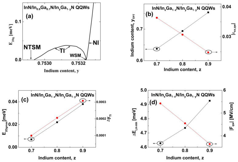
In this study, we present a theoretical study of the quantum spin Hall effect in InN/InGaN coupled multiple quantum wells with the individual well widths equal to two atomic monolayers. We consider triple and quadruple quantum wells in which the In content in the interwell barriers is greater than or equal to the In content in the external barriers. To calculate the electronic subbands in these nanostructures, we use the eight-band Hamiltonian, assuming that the effective spin-orbit interaction in InN is negative, which represents the worst-case scenario for achieving a two-dimensional topological insulator. For triple quantum wells, we find that when the In contents of the external and interwell barriers are the same and the widths of the internal barriers are equal to two monolayers, a topological insulator with a bulk energy gap of 0.25 meV can appear. Increasing the In content in the interwell barriers leads to a significant increase in the bulk energy gap of the topological insulator, reaching about 0.8 meV. In these structures, the topological insulator can be achieved when the In content in the external barriers is about 0.64, causing relatively low strain in quantum wells and making the epitaxial growth of these structures within the range of current technology. Using the effective 2D Hamiltonian, we study the edge states in strip structures containing topological triple quantum wells. We demonstrate that the opening of the gap in the spectrum of the edge states caused by decreasing the width of the strip has an oscillatory character regardless of whether the pseudospin-mixing elements of the effective Hamiltonian are omitted or taken into account. The strength of the finite size effect in these structures is several times smaller than that in HgTe/HgCdTe and InAs/GaSb/AlSb topological insulators. Therefore, its influence on the quantum spin Hall effect is negligible in strips with a width larger than 150 nm, unless the temperature at which electron transport is measured is less than 1 mK. In the case of quadruple quantum wells, we find the topological insulator phase only when the In content in the interwell barriers is larger than in the external barriers. We show that in these structures, a topological insulator with a bulk energy gap of 0.038 meV can be achieved when the In content in the external barriers is about 0.75. Since this value of the bulk energy gap is very small, quadruple quantum wells are less useful for realizing a measurable quantum spin Hall system, but they are still attractive for achieving a topological phase transition and a nonlocal topological semimetal phase.
在本研究中,我们对阱宽均为两个原子单层的InN/InGaN耦合多量子阱中的量子自旋霍尔效应进行了理论研究。我们考虑了阱间势垒中In含量大于或等于外部势垒中In含量的三量子阱和四量子阱。为了计算这些纳米结构中的电子子带,我们使用八能带哈密顿量,假设InN中的有效自旋轨道相互作用为负,这代表了实现二维拓扑绝缘体的最坏情况。对于三量子阱,我们发现当外部和阱间势垒的In含量相同时且内部势垒宽度等于两个单层时,可能会出现体能隙为0.25 meV的拓扑绝缘体。增加阱间势垒中的In含量会导致拓扑绝缘体的体能隙显著增加,达到约0.8 meV。在这些结构中,当外部势垒中的In含量约为0.64时可实现拓扑绝缘体,这会在量子阱中产生相对较低的应变,并使这些结构在当前技术范围内实现外延生长。使用有效的二维哈密顿量,我们研究了包含拓扑三量子阱的条形结构中的边缘态。我们证明,无论有效哈密顿量的赝自旋混合元素是否被忽略或考虑在内由减小条形宽度引起的边缘态能谱中的能隙打开都具有振荡特性。这些结构中的有限尺寸效应强度比HgTe/HgCdTe和InAs/GaSb/AlSb拓扑绝缘体中的小几倍。因此,除非测量电子输运的温度低于1 mK,否则其对宽度大于150 nm的条形结构中的量子自旋霍尔效应的影响可忽略不计。对于四量子阱,我们仅在阱间势垒中的In含量大于外部势垒中的In含量时才发现拓扑绝缘体相。我们表明,在这些结构中,当外部势垒中的In含量约为0.75时可实现体能隙为0.038 meV的拓扑绝缘体。由于这个体能隙值非常小,四量子阱对于实现可测量的量子自旋霍尔系统用处较小,但它们对于实现拓扑相变和非局域拓扑半金属相仍然具有吸引力。