Nir-Harwood Rivka-Galya, Cohen Guy, Majumdar Amlan, Haight Richard, Ber Emanuel, Gignac Lynne, Ordan Efrat, Shoham Lishai, Keller Yair, Kornblum Lior, Yalon Eilam
Viterbi Faculty of Electrical & Computer Engineering, Technion-Israel Institute of Technology, Haifa 32000, Israel.
IBM Thomas J. Watson Research Center, Yorktown Heights, New York 10598, United States.
ACS Nano. 2024 Mar 19;18(11):8029-8037. doi: 10.1021/acsnano.3c11019. Epub 2024 Mar 8.
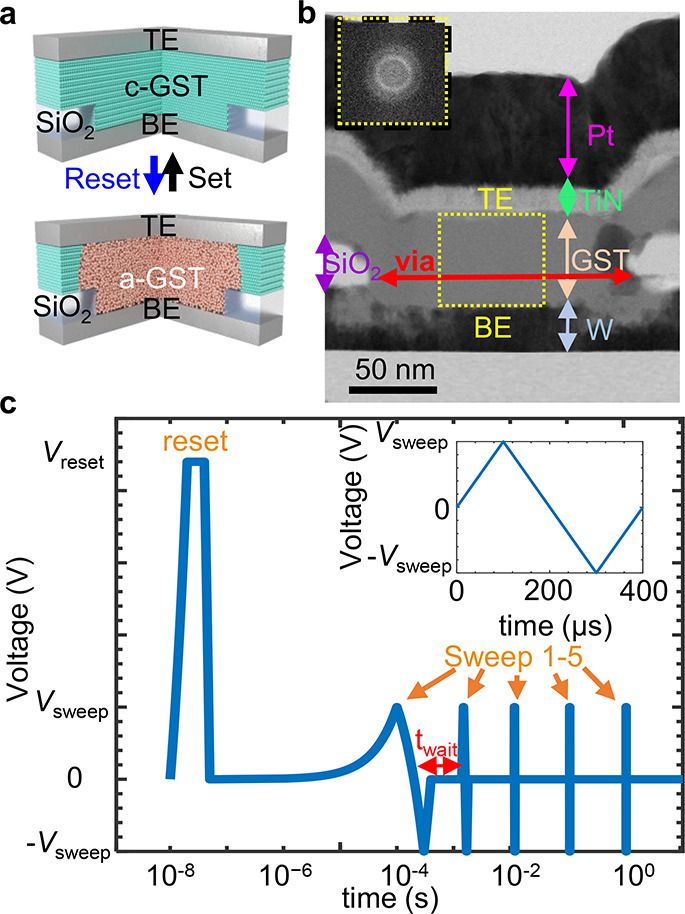
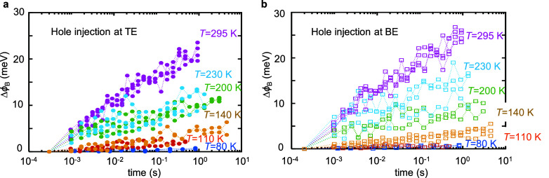
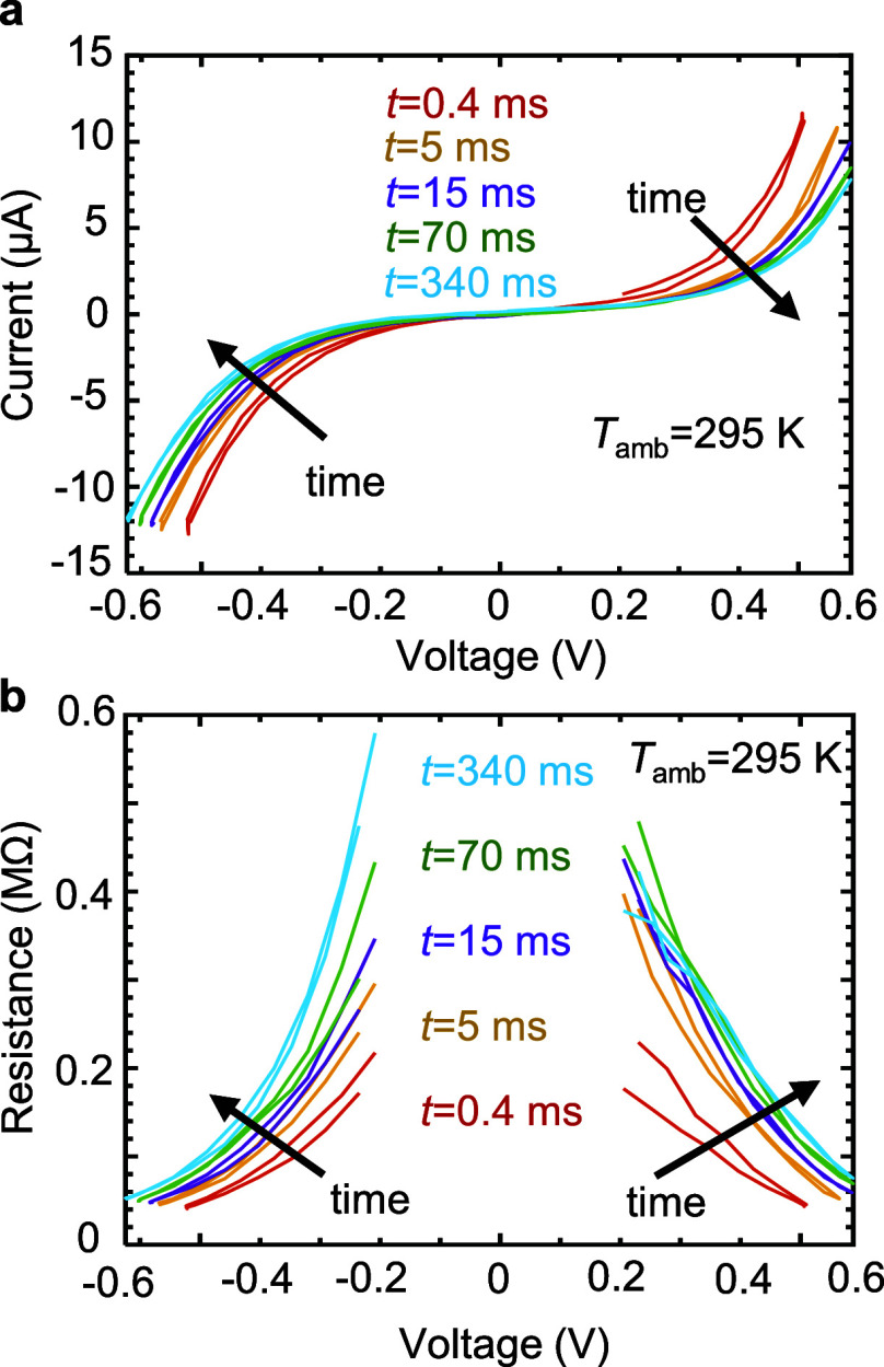
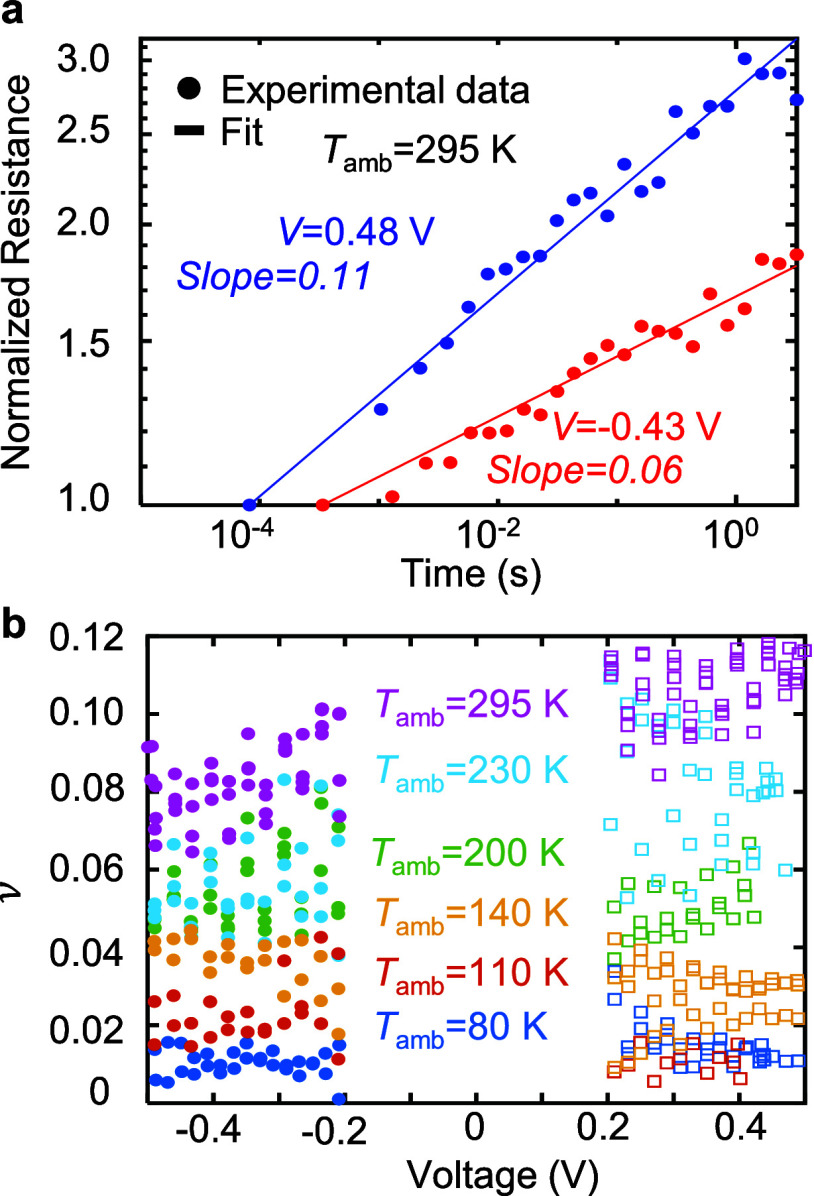
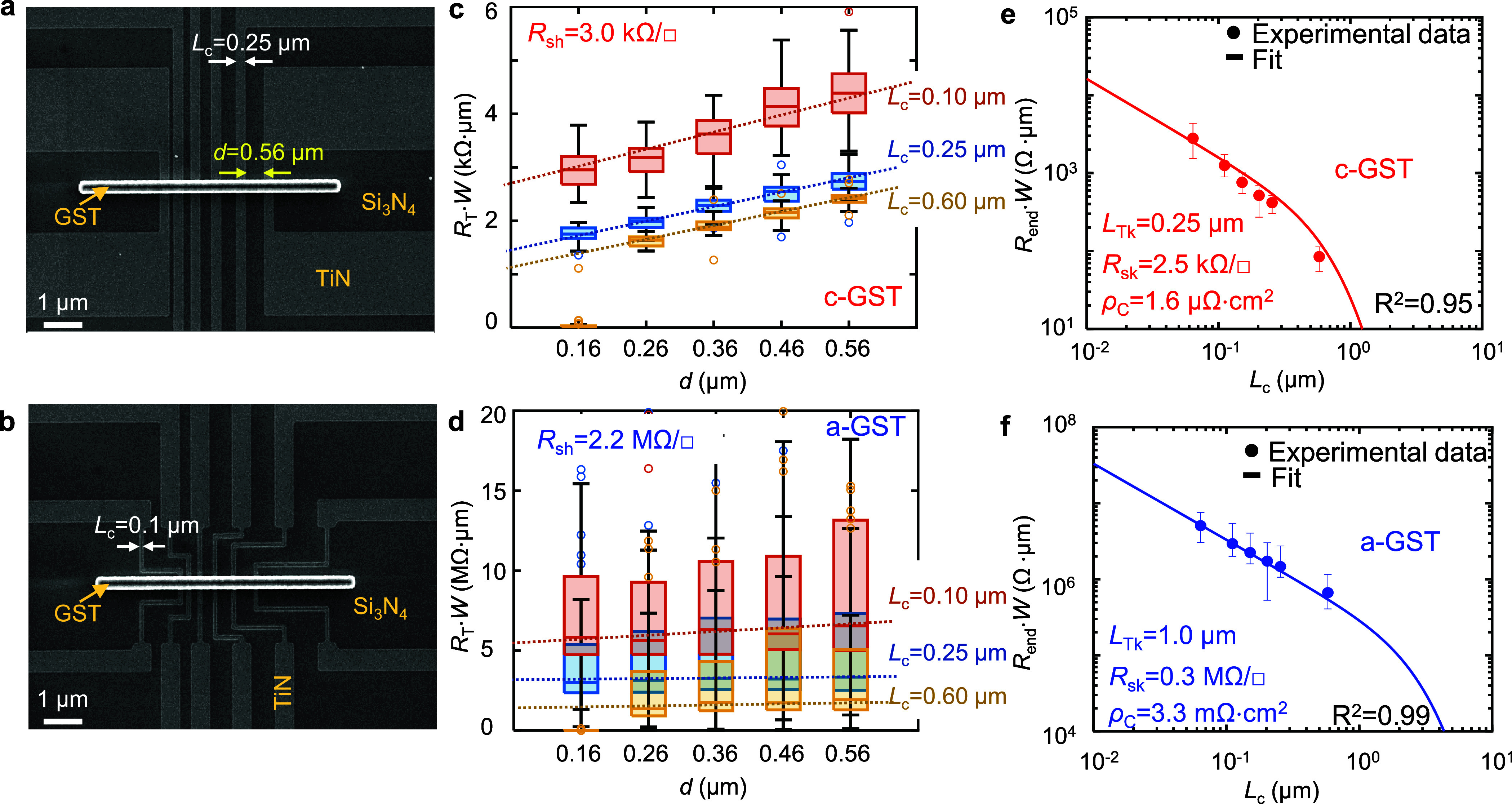
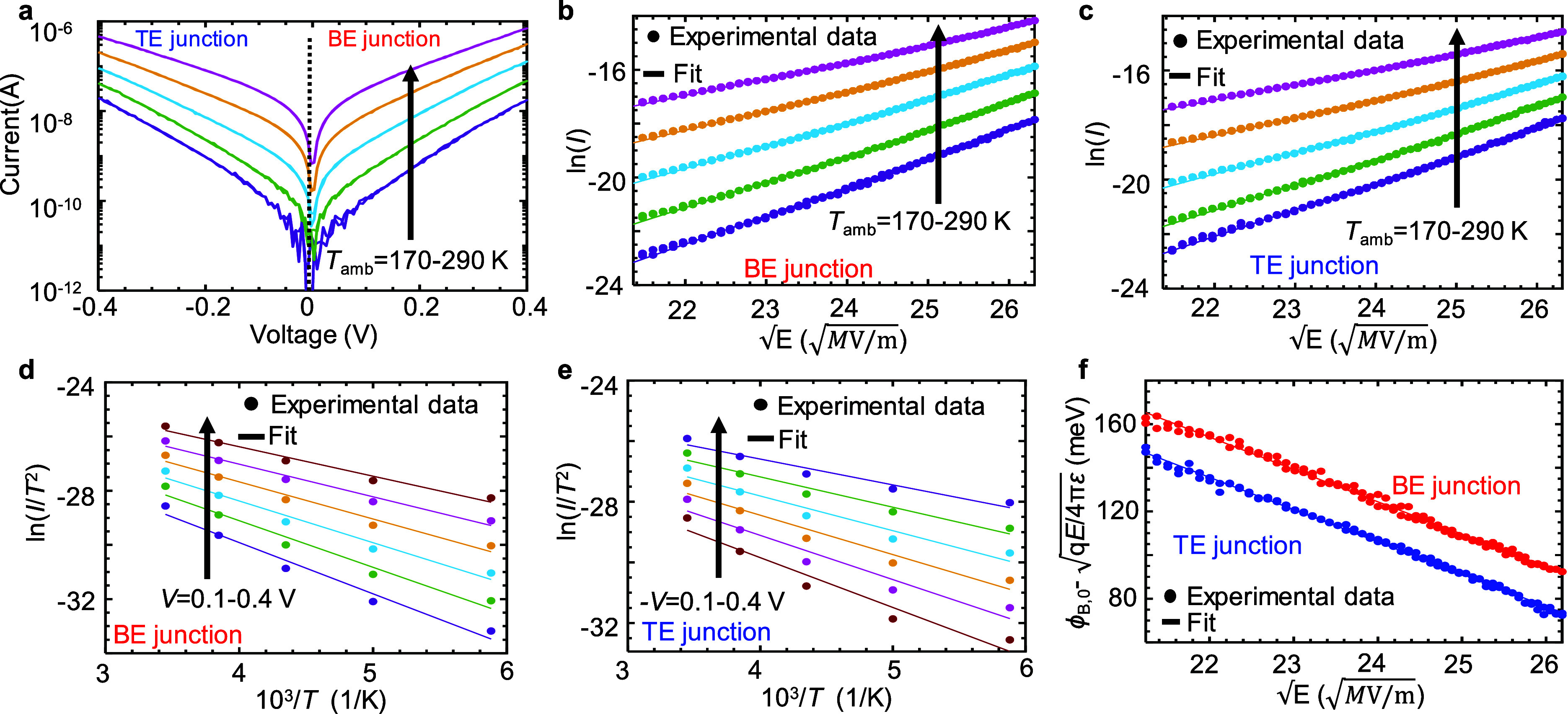
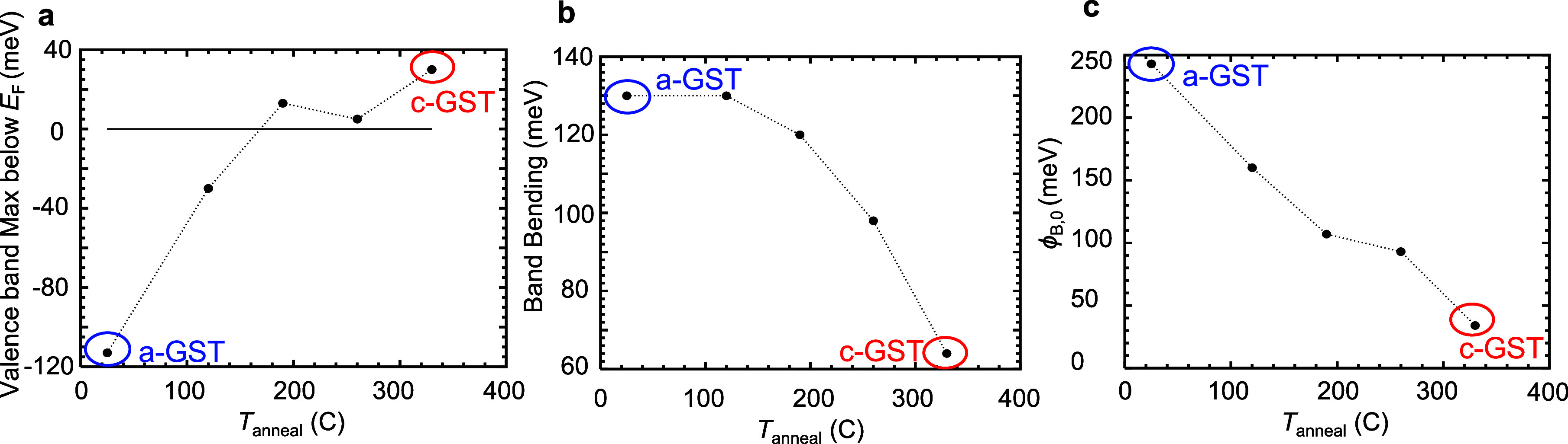
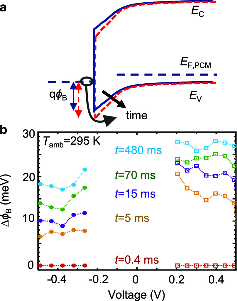
Phase-change memory (PCM) devices have great potential as multilevel memory cells and artificial synapses for neuromorphic computing hardware. However, their practical use is hampered by resistance drift, a phenomenon commonly attributed to structural relaxation or electronic mechanisms primarily in the context of bulk effects. In this study, we reevaluate the electrical manifestation of resistance drift in sub-100 nm GeSbTe (GST) PCM devices, focusing on the contributions of bulk vs interface effects. We employ a combination of measurement techniques to elucidate the current transport mechanism and the electrical manifestation of resistance drift. Our steady-state temperature-dependent measurements reveal that resistance in these devices is predominantly influenced by their electrical contacts, with conduction occurring through thermionic emission (Schottky) at the contacts. Additionally, temporal current-voltage characterization allows us to link the resistance drift to a time-dependent increase in the Schottky barrier height. These findings provide valuable insights, pinpointing the primary contributor to resistance drift in PCM devices: the Schottky barrier height for hole injection at the interface. This underscores the significance of contacts (interface) in the electrical manifestation of drift in PCM devices.
相变存储器(PCM)器件作为用于神经形态计算硬件的多级存储单元和人工突触具有巨大潜力。然而,其实际应用受到电阻漂移的阻碍,这种现象通常主要在体效应的背景下归因于结构弛豫或电子机制。在本研究中,我们重新评估了亚100纳米锗锑碲(GST)PCM器件中电阻漂移的电学表现,重点关注体效应与界面效应的贡献。我们采用多种测量技术来阐明电流传输机制和电阻漂移的电学表现。我们的稳态温度相关测量表明,这些器件中的电阻主要受其电接触的影响,传导通过接触处的热电子发射(肖特基)发生。此外,时间相关的电流 - 电压表征使我们能够将电阻漂移与肖特基势垒高度随时间的增加联系起来。这些发现提供了有价值的见解,确定了PCM器件中电阻漂移的主要贡献因素:界面处空穴注入的肖特基势垒高度。这突出了接触(界面)在PCM器件漂移电学表现中的重要性。