Bok Ilhan, Ashtiani Alireza, Gokhale Yash, Phillips Jack, Zhu Tianxiang, Hai Aviad
Department of Biomedical Engineering, University of Wisconsin-Madison, Madison, WI USA.
Department of Electrical and Computer Engineering, University of Wisconsin-Madison, Madison, WI USA.
Microsyst Nanoeng. 2024 Mar 25;10:44. doi: 10.1038/s41378-024-00674-9. eCollection 2024.
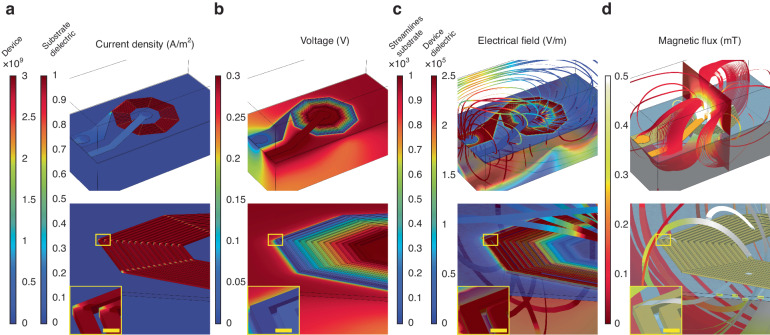
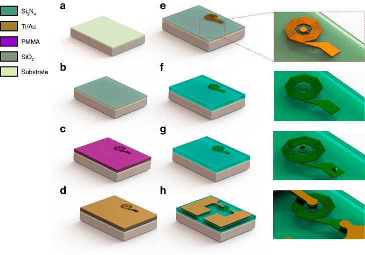
Circuit-integrated electromagnets are fundamental building blocks for on-chip signal transduction, modulation, and tunability, with specific applications in environmental and biomedical micromagnetometry. A primary challenge for improving performance is pushing quality limitations while minimizing size and fabrication complexity and retaining spatial capabilities. Recent efforts have exploited highly involved three-dimensional synthesis, advanced insulation, and exotic material compositions. Here, we present a rapid nanofabrication process that employs electron beam dose control for high-turn-density diamond-embedded flat spiral coils; these coils achieve efficient on-chip electromagnetic-to-optical signal conversion. Our fabrication process relies on fast 12.3 s direct writing on standard poly(methyl methacrylate) as a basis for the metal lift-off process. Prototypes with 70 micrometer overall diameters and 49-470 nm interturn spacings with corresponding inductances of 12.3-12.8 nH are developed. We utilize optical micromagnetometry to demonstrate that magnetic field generation at the center of the structure effectively correlates with finite element modeling predictions. Further designs based on our process can be integrated with photolithography to broadly enable optical magnetic sensing and spin-based computation.
电路集成电磁铁是片上信号转导、调制和可调性的基本构建模块,在环境和生物医学微磁测量中有特定应用。提高性能的一个主要挑战是在最小化尺寸和制造复杂性并保持空间能力的同时突破质量限制。最近的努力采用了高度复杂的三维合成、先进的绝缘和奇特的材料成分。在这里,我们展示了一种快速纳米制造工艺,该工艺采用电子束剂量控制来制造高匝数密度的嵌入式金刚石平面螺旋线圈;这些线圈实现了高效的片上电磁到光信号转换。我们的制造工艺基于在标准聚甲基丙烯酸甲酯上快速进行12.3秒的直接写入,作为金属剥离工艺的基础。开发了整体直径为70微米、匝间距为49 - 470纳米且相应电感为12.3 - 12.8纳亨的原型。我们利用光学微磁测量来证明结构中心处的磁场产生与有限元建模预测有效相关。基于我们工艺的进一步设计可以与光刻技术集成,从而广泛实现光学磁传感和基于自旋的计算。