• 文献检索
  • 文档翻译
  • 深度研究
  • 学术资讯
  • Suppr Zotero 插件Zotero 插件
  • 邀请有礼
  • 套餐&价格
  • 历史记录
应用&插件
Suppr Zotero 插件Zotero 插件浏览器插件Mac 客户端Windows 客户端微信小程序
定价
高级版会员购买积分包购买API积分包
服务
文献检索文档翻译深度研究API 文档MCP 服务
关于我们
关于 Suppr公司介绍联系我们用户协议隐私条款
关注我们

Suppr 超能文献

核心技术专利:CN118964589B侵权必究
粤ICP备2023148730 号-1Suppr @ 2026

文献检索

告别复杂PubMed语法,用中文像聊天一样搜索,搜遍4000万医学文献。AI智能推荐,让科研检索更轻松。

立即免费搜索

文件翻译

保留排版,准确专业,支持PDF/Word/PPT等文件格式,支持 12+语言互译。

免费翻译文档

深度研究

AI帮你快速写综述,25分钟生成高质量综述,智能提取关键信息,辅助科研写作。

立即免费体验

磷和锑掺杂对在硅上生长的锗薄层的影响。

Effects of phosphorous and antimony doping on thin Ge layers grown on Si.

作者信息

Yu Xueying, Jia Hui, Yang Junjie, Masteghin Mateus G, Beere Harvey, Mtunzi Makhayeni, Deng Huiwen, Huo Suguo, Chen Chong, Chen Siming, Tang Mingchu, Sweeney Stephen J, Ritchie David, Seeds Alwyn, Liu Huiyun

机构信息

Department of Electronic and Electrical Engineering, University College London, Torrington Place, London, WC1E 7JE, UK.

Advanced Technology Institute, University of Surrey, Guildford, Surrey, GU2 7XH, UK.

出版信息

Sci Rep. 2024 Apr 4;14(1):7969. doi: 10.1038/s41598-024-57937-8.

DOI:10.1038/s41598-024-57937-8
PMID:38575676
原文链接:https://pmc.ncbi.nlm.nih.gov/articles/PMC10995153/
Abstract

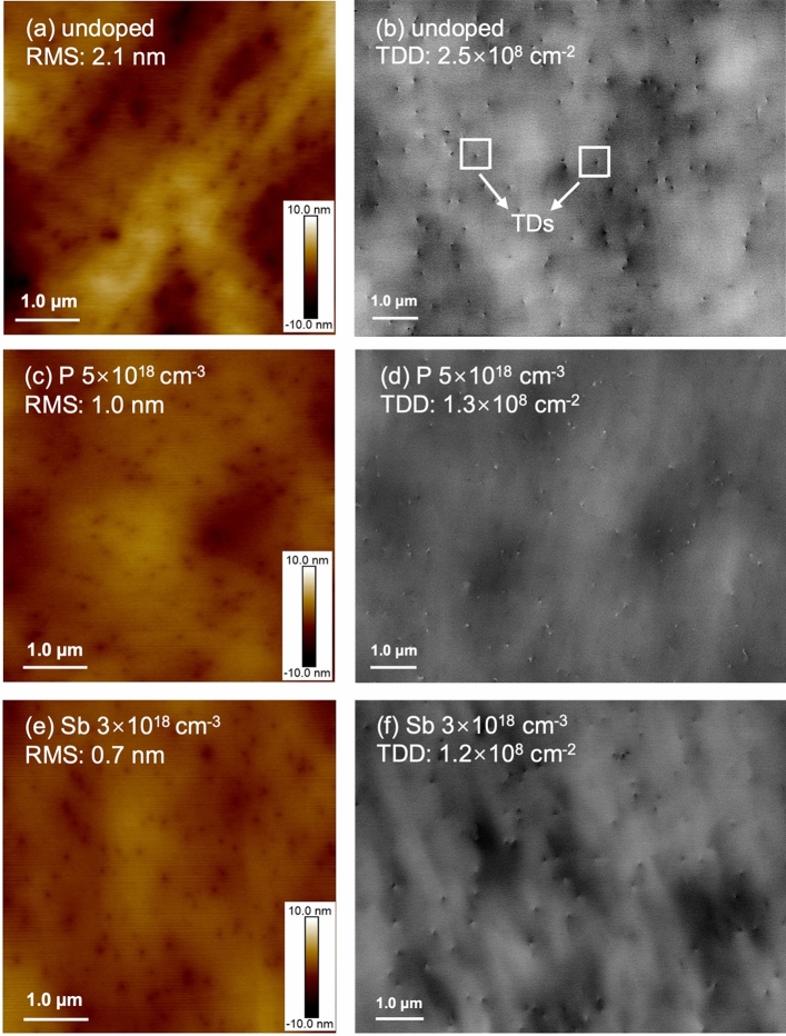
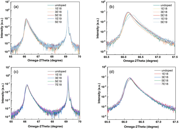
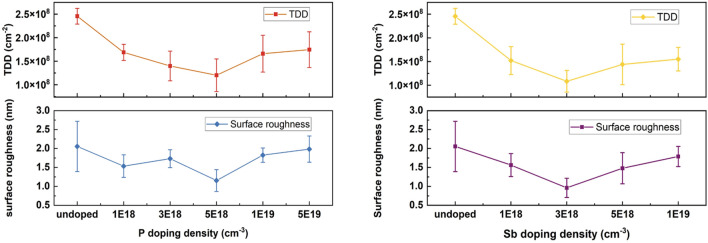
Suppression of threading dislocations (TDs) in thin germanium (Ge) layers grown on silicon (Si) substrates has been critical for realizing high-performance Si-based optoelectronic and electronic devices. An advanced growth strategy is desired to minimize the TD density within a thin Ge buffer layer in Ge-on-Si systems. In this work, we investigate the impact of P dopants in 500-nm thin Ge layers, with doping concentrations from 1 to 50 × 10 cm. The introduction of P dopants has efficiently promoted TD reduction, whose potential mechanism has been explored by comparing it to the well-established Sb-doped Ge-on-Si system. P and Sb dopants reveal different defect-suppression mechanisms in Ge-on-Si samples, inspiring a novel co-doping technique by exploiting the advantages of both dopants. The surface TDD of the Ge buffer has been further reduced by the co-doping technique to the order of 10 cm with a thin Ge layer (of only 500 nm), which could provide a high-quality platform for high-performance Si-based semiconductor devices.

摘要

抑制在硅(Si)衬底上生长的锗(Ge)薄层中的穿透位错(TDs)对于实现高性能的硅基光电器件和电子器件至关重要。需要一种先进的生长策略来最小化Ge-on-Si系统中薄Ge缓冲层内的TD密度。在这项工作中,我们研究了磷(P)掺杂剂对500纳米厚的Ge层的影响,其掺杂浓度范围为1至50×10¹⁹厘米⁻³。P掺杂剂的引入有效地促进了TD的减少,通过将其与成熟的Sb掺杂的Ge-on-Si系统进行比较,探索了其潜在机制。P和Sb掺杂剂在Ge-on-Si样品中揭示了不同的缺陷抑制机制,通过利用两种掺杂剂的优点激发了一种新型的共掺杂技术。通过共掺杂技术,Ge缓冲层的表面TDD进一步降低到10¹⁰厘米⁻²的量级,使用的是仅500纳米厚的Ge薄层,这可以为高性能硅基半导体器件提供一个高质量的平台。

https://cdn.ncbi.nlm.nih.gov/pmc/blobs/77d6/10995153/16b6edd1e3ea/41598_2024_57937_Fig4_HTML.jpg
https://cdn.ncbi.nlm.nih.gov/pmc/blobs/77d6/10995153/bcf51b82c0db/41598_2024_57937_Fig2_HTML.jpg
https://cdn.ncbi.nlm.nih.gov/pmc/blobs/77d6/10995153/f5bd8ff51fba/41598_2024_57937_Fig3_HTML.jpg
https://cdn.ncbi.nlm.nih.gov/pmc/blobs/77d6/10995153/16b6edd1e3ea/41598_2024_57937_Fig4_HTML.jpg
https://cdn.ncbi.nlm.nih.gov/pmc/blobs/77d6/10995153/bcf51b82c0db/41598_2024_57937_Fig2_HTML.jpg
https://cdn.ncbi.nlm.nih.gov/pmc/blobs/77d6/10995153/f5bd8ff51fba/41598_2024_57937_Fig3_HTML.jpg
https://cdn.ncbi.nlm.nih.gov/pmc/blobs/77d6/10995153/16b6edd1e3ea/41598_2024_57937_Fig4_HTML.jpg

相似文献

1
Effects of phosphorous and antimony doping on thin Ge layers grown on Si.磷和锑掺杂对在硅上生长的锗薄层的影响。
Sci Rep. 2024 Apr 4;14(1):7969. doi: 10.1038/s41598-024-57937-8.
2
Theoretical Calculation and Experimental Verification for Dislocation Reduction in Germanium Epitaxial Layers with Semicylindrical Voids on Silicon.
J Vis Exp. 2020 Jul 17(161). doi: 10.3791/58897.
3
Vertically oriented epitaxial germanium nanowires on silicon substrates using thin germanium buffer layers.硅衬底上使用薄锗缓冲层的垂直取向外延锗纳米线。
Nanotechnology. 2010 Jul 23;21(29):295602. doi: 10.1088/0957-4484/21/29/295602. Epub 2010 Jun 29.
4
Low-power and high-detectivity Ge photodiodes by in-situ heavy As doping during Ge-on-Si seed layer growth.通过在硅基锗籽晶层生长过程中原位重掺杂砷制备的低功耗高探测率锗光电二极管。
Opt Express. 2021 Feb 1;29(3):2940-2952. doi: 10.1364/OE.405364.
5
Role of Metallic Adlayer in Limiting Ge Incorporation into GaN.金属粘附层在限制锗掺入氮化镓中的作用。
Materials (Basel). 2022 Aug 27;15(17):5929. doi: 10.3390/ma15175929.
6
Reduced Dislocation of GaAs Layer Grown on Ge-Buffered Si (001) Substrate Using Dislocation Filter Layers for an O-Band InAs/GaAs Quantum Dot Narrow-Ridge Laser.使用位错过滤层在锗缓冲硅(001)衬底上生长的砷化镓层的位错减少,用于O波段砷化铟/砷化镓量子点窄脊激光器。
Micromachines (Basel). 2022 Sep 22;13(10):1579. doi: 10.3390/mi13101579.
7
Enhanced direct-gap light emission from Si-capped n-Ge epitaxial layers on Si after post-growth rapid cyclic annealing: impact of non-radiative interface recombination toward Ge/Si double heterostructure lasers.生长后快速循环退火后,硅帽n-Ge外延层在硅上增强的直接带隙光发射:非辐射界面复合对Ge/Si双异质结构激光器的影响。
Opt Express. 2017 Sep 4;25(18):21286-21300. doi: 10.1364/OE.25.021286.
8
Photodetection in Hybrid Single-Layer Graphene/Fully Coherent Germanium Island Nanostructures Selectively Grown on Silicon Nanotip Patterns.在选择性地生长于硅纳米尖图案上的混合单层石墨烯/完全相干锗岛纳米结构中进行光探测。
ACS Appl Mater Interfaces. 2016 Jan 27;8(3):2017-26. doi: 10.1021/acsami.5b10336. Epub 2016 Jan 13.
9
Shallow Heavily Doped n++ Germanium by Organo-Antimony Monolayer Doping.有机-锑单层掺杂实现浅且重掺杂 n++ 型锗。
ACS Appl Mater Interfaces. 2017 Jun 14;9(23):20179-20187. doi: 10.1021/acsami.7b02645. Epub 2017 Jun 5.
10
X-ray characterization of Ge dots epitaxially grown on nanostructured Si islands on silicon-on-insulator substrates.绝缘体上硅衬底上纳米结构硅岛外延生长的锗点的X射线表征
J Appl Crystallogr. 2013 Aug 1;46(Pt 4):868-873. doi: 10.1107/S0021889813003518. Epub 2013 Jun 7.

本文引用的文献

1
InAs/GaAs quantum-dot lasers grown on on-axis Si (001) without dislocation filter layers.在没有位错过滤层的轴向 Si(001)上生长的 InAs/GaAs 量子点激光器。
Opt Express. 2023 Jan 30;31(3):4862-4872. doi: 10.1364/OE.475976.
2
From past to future: on-chip laser sources for photonic integrated circuits.从过去到未来:用于光子集成电路的片上激光源。
Light Sci Appl. 2023 Jan 15;12(1):16. doi: 10.1038/s41377-022-01006-0.
3
Prospects and applications of on-chip lasers.片上激光器的前景与应用
eLight. 2023;3(1):1. doi: 10.1186/s43593-022-00027-x. Epub 2023 Jan 4.
4
High-Performance Waveguide-Integrated Ge/Si Avalanche Photodetector with Lateral Multiplication Region.具有横向倍增区的高性能波导集成锗/硅雪崩光电探测器。
Micromachines (Basel). 2022 Apr 19;13(5):649. doi: 10.3390/mi13050649.
5
Dual-Step Selective Homoepitaxy of Ge with Low Defect Density and Modulated Strain Based on Optimized Ge/Si Virtual Substrate.基于优化的Ge/Si虚拟衬底的具有低缺陷密度和调制应变的锗双步选择性同质外延
Materials (Basel). 2022 May 18;15(10):3594. doi: 10.3390/ma15103594.
6
Strain Modulation of Selectively and/or Globally Grown Ge Layers.选择性生长和/或整体生长的锗层的应变调制
Nanomaterials (Basel). 2021 May 28;11(6):1421. doi: 10.3390/nano11061421.
7
Nanophotonic Pockels modulators on a silicon nitride platform.基于氮化硅平台的纳米光子学普克尔调制器。
Nat Commun. 2018 Aug 27;9(1):3444. doi: 10.1038/s41467-018-05846-6.
8
All MBE grown InAs/GaAs quantum dot lasers on on-axis Si (001).所有分子束外延生长的InAs/GaAs量子点激光器均位于轴向Si(001)上。
Opt Express. 2018 Apr 30;26(9):11568-11576. doi: 10.1364/OE.26.011568.
9
1.3-μm InAs/GaAs quantum-dot lasers monolithically grown on Si substrates using InAlAs/GaAs dislocation filter layers.使用InAlAs/GaAs位错过滤层在硅衬底上单片生长的1.3微米InAs/GaAs量子点激光器。
Opt Express. 2014 May 19;22(10):11528-35. doi: 10.1364/OE.22.011528.
10
Point defect engineering strategies to retard phosphorous diffusion in germanium.点缺陷工程策略延缓磷在锗中的扩散。
Phys Chem Chem Phys. 2013 Jan 7;15(1):367-71. doi: 10.1039/c2cp42973j. Epub 2012 Nov 21.