Feng Ganrong, Li Shan, Tian Yawen, Qi Song, Guo Daoyou, Tang Weihua
College of Integrated Circuit Science and Engineering & National and Local Joint Engineering Laboratory for RF Integration and Micro-Packing Technologies, Nanjing University of Posts and Telecommunications, Nanjing 210023, China.
Beijing GAO Semiconductor Co. Ltd., Beijing 101407, China.
ACS Omega. 2024 Apr 24;9(20):22084-22089. doi: 10.1021/acsomega.4c00405. eCollection 2024 May 21.
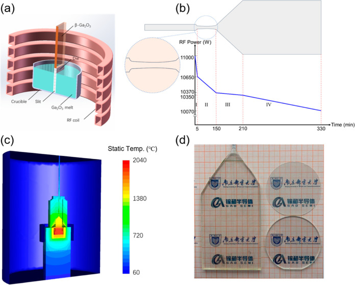
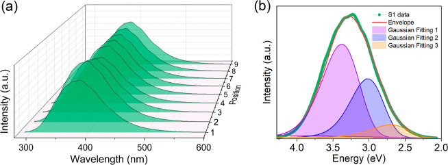
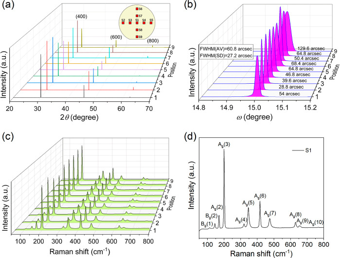
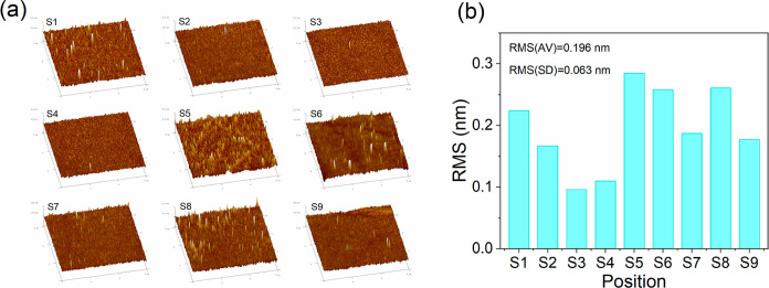
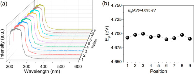
2 in. bulk β-GaO single crystals are successfully grown by the edge-defined film-fed growth method with a homemade furnace system. By considering the significance of wafer quality in future mass manufacture, a nine-point characterization method is developed to evaluate the full-scale quality of the processed 2 in. (100)-orientated β-GaO single-crystal wafers. Crystalline and structural characteristics were evaluated using X-ray diffraction and Raman spectroscopy, revealing decent crystalline quality with a mean full width at half-maximum value of 60.8 arcsec and homogeneous bonding structures. The statistical root-mean-square surface roughness, determined from nine scanning areas, was found to be only 0.196 nm, indicating superior surface quality. Linear optical properties and defect levels were further investigated using UV-visible spectrophotometry and photoluminescence spectroscopy. The high wafer-scale quality of the processed β-GaO wafers meets the requirements for homoepitaxial growth substrates in electronic and photonic devices with vertical configurations.
采用自制炉体系统,通过边缘限定膜进给生长法成功生长出了2英寸块状β-GaO单晶。考虑到晶圆质量在未来大规模制造中的重要性,开发了一种九点表征方法来评估加工后的2英寸(100)取向β-GaO单晶晶圆的全面质量。使用X射线衍射和拉曼光谱对晶体和结构特性进行了评估,结果表明晶体质量良好,半高宽平均值为60.8角秒,键合结构均匀。从九个扫描区域确定的统计均方根表面粗糙度仅为0.196nm,表明表面质量优异。使用紫外-可见分光光度法和光致发光光谱进一步研究了线性光学性质和缺陷能级。加工后的β-GaO晶圆具有很高的晶圆尺度质量,满足了垂直结构电子和光子器件中外延生长衬底的要求。