• 文献检索
  • 文档翻译
  • 深度研究
  • 学术资讯
  • Suppr Zotero 插件Zotero 插件
  • 邀请有礼
  • 套餐&价格
  • 历史记录
应用&插件
Suppr Zotero 插件Zotero 插件浏览器插件Mac 客户端Windows 客户端微信小程序
定价
高级版会员购买积分包购买API积分包
服务
文献检索文档翻译深度研究API 文档MCP 服务
关于我们
关于 Suppr公司介绍联系我们用户协议隐私条款
关注我们

Suppr 超能文献

核心技术专利:CN118964589B侵权必究
粤ICP备2023148730 号-1Suppr @ 2026

文献检索

告别复杂PubMed语法,用中文像聊天一样搜索,搜遍4000万医学文献。AI智能推荐,让科研检索更轻松。

立即免费搜索

文件翻译

保留排版,准确专业,支持PDF/Word/PPT等文件格式,支持 12+语言互译。

免费翻译文档

深度研究

AI帮你快速写综述,25分钟生成高质量综述,智能提取关键信息,辅助科研写作。

立即免费体验

边缘限定膜进给生长中β-GaO单晶的预熔化辅助杂质控制

Pre-Melting-Assisted Impurity Control of β-GaO Single Crystals in Edge-Defined Film-Fed Growth.

作者信息

Shin A-Ran, Gu Tae-Hun, Shin Yun-Ji, Jeong Seong-Min, Lee Heesoo, Bae Si-Young

机构信息

Semiconductor Materials Center, Korea Institute of Ceramic Engineering and Technology, Jinju 52851, Republic of Korea.

School of Materials Science and Engineering, Pusan National University, Busan 46241, Republic of Korea.

出版信息

Nanomaterials (Basel). 2024 Dec 25;15(1):7. doi: 10.3390/nano15010007.

DOI:10.3390/nano15010007
PMID:39791767
原文链接:https://pmc.ncbi.nlm.nih.gov/articles/PMC11722084/
Abstract

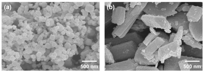
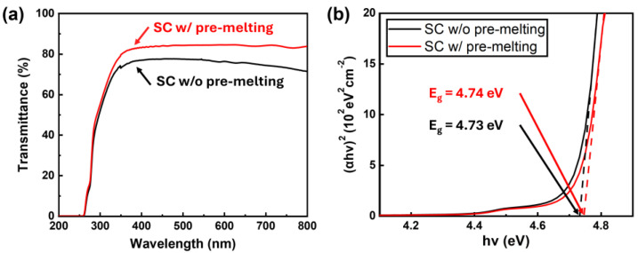
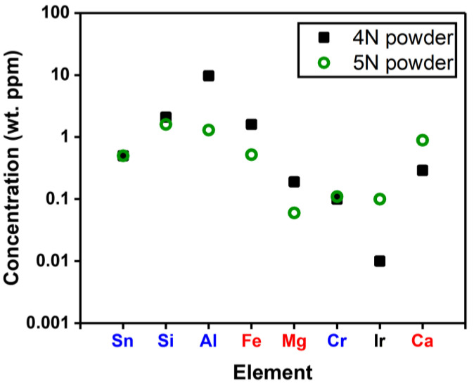
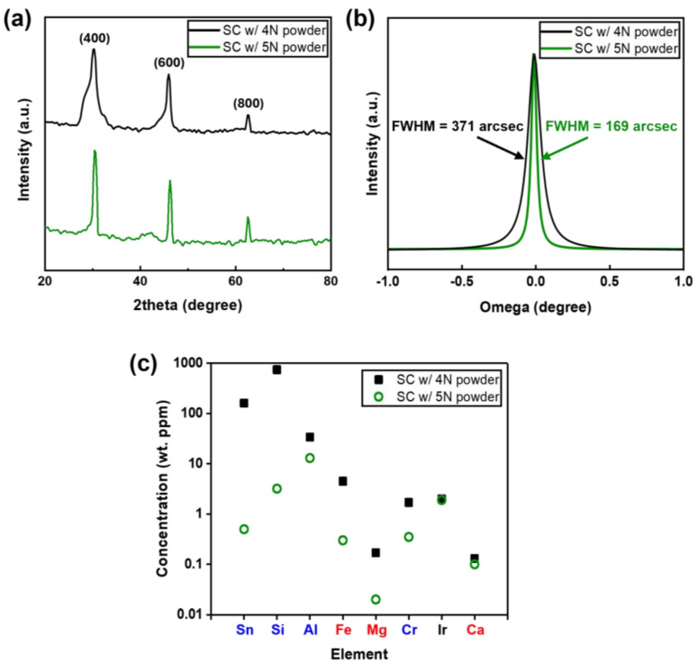
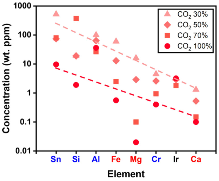
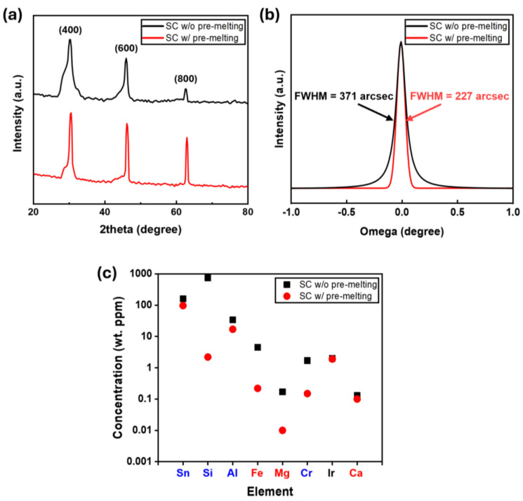
This study reveals the significant role of the pre-melting process in growing high-quality (100) β-GaO single crystals from 4N powder (99.995% purity) using the edge-defined film-fed growth (EFG) method. Among various bulk melt growth methods, the EFG method boasts a fast growth rate and the capability of growing multiple crystals simultaneously, thus offering high productivity. The pre-melting process notably enhanced the structural, optical, and electrical properties of the crystals by effectively eliminating impurities such as Si and Fe. Specifically, employing a 100% CO atmosphere during pre-melting proved to be highly effective, reducing impurity concentrations and carrier scattering, which resulted in a decreased carrier concentration and an increased electron mobility in the grown GaO single crystals. These results demonstrate that pre-melting is a crucial technique for substantially improving crystal quality, thereby promising better performance in β-GaO-based device applications.

摘要

本研究揭示了预熔过程在使用边缘限定膜进给生长(EFG)方法从4N粉末(纯度99.995%)生长高质量(100)β-GaO单晶中的重要作用。在各种体熔体生长方法中,EFG方法具有生长速度快和能够同时生长多个晶体的能力,因此具有高生产率。预熔过程通过有效去除Si和Fe等杂质,显著提高了晶体的结构、光学和电学性能。具体而言,在预熔过程中采用100%的CO气氛被证明是非常有效的,降低了杂质浓度和载流子散射,这导致生长的GaO单晶中的载流子浓度降低和电子迁移率增加。这些结果表明,预熔是大幅提高晶体质量的关键技术,从而有望在基于β-GaO的器件应用中实现更好的性能。

https://cdn.ncbi.nlm.nih.gov/pmc/blobs/24fd/11722084/f69768b12ad8/nanomaterials-15-00007-g006.jpg
https://cdn.ncbi.nlm.nih.gov/pmc/blobs/24fd/11722084/4af92921b41c/nanomaterials-15-00007-g001.jpg
https://cdn.ncbi.nlm.nih.gov/pmc/blobs/24fd/11722084/9a75575c82f8/nanomaterials-15-00007-g002.jpg
https://cdn.ncbi.nlm.nih.gov/pmc/blobs/24fd/11722084/3381b02f453d/nanomaterials-15-00007-g003.jpg
https://cdn.ncbi.nlm.nih.gov/pmc/blobs/24fd/11722084/1cf330265dc5/nanomaterials-15-00007-g004.jpg
https://cdn.ncbi.nlm.nih.gov/pmc/blobs/24fd/11722084/3804e022886a/nanomaterials-15-00007-g005.jpg
https://cdn.ncbi.nlm.nih.gov/pmc/blobs/24fd/11722084/f69768b12ad8/nanomaterials-15-00007-g006.jpg

相似文献

1
Pre-Melting-Assisted Impurity Control of β-GaO Single Crystals in Edge-Defined Film-Fed Growth.边缘限定膜进给生长中β-GaO单晶的预熔化辅助杂质控制
Nanomaterials (Basel). 2024 Dec 25;15(1):7. doi: 10.3390/nano15010007.
2
Growth of bulk β-GaO crystals from melt without precious-metal crucible by pulling from a cold container.通过从冷容器提拉法在无贵金属坩埚的情况下从熔体中生长块状β-GaO晶体。
Sci Rep. 2024 Jun 27;14(1):14881. doi: 10.1038/s41598-024-65420-7.
3
2 in. Bulk β-GaO Single Crystals Grown by EFG Method with High Wafer-Scale Quality.采用EFG法生长的具有高晶圆级质量的2英寸块状β-GaO单晶。
ACS Omega. 2024 Apr 24;9(20):22084-22089. doi: 10.1021/acsomega.4c00405. eCollection 2024 May 21.
4
Scintillation and radioluminescence mechanism in β-GaO semiconducting single crystals.β-GaO 半导体单晶中的闪烁和辐射发光机制。
Heliyon. 2023 Oct 26;9(11):e21240. doi: 10.1016/j.heliyon.2023.e21240. eCollection 2023 Nov.
5
Composition and Surface Optical Properties of GaSe:Eu Crystals before and after Heat Treatment.热处理前后GaSe:Eu晶体的组成与表面光学性质
Materials (Basel). 2024 Jan 13;17(2):405. doi: 10.3390/ma17020405.
6
Low Thermal Budget Heteroepitaxial Gallium Oxide Thin Films Enabled by Atomic Layer Deposition.通过原子层沉积实现的低热预算异质外延氧化镓薄膜
ACS Appl Mater Interfaces. 2020 Sep 30;12(39):44225-44237. doi: 10.1021/acsami.0c08477. Epub 2020 Sep 15.
7
Electrical Characterizations of Planar GaO Schottky Barrier Diodes.平面GaO肖特基势垒二极管的电学特性
Micromachines (Basel). 2021 Mar 3;12(3):259. doi: 10.3390/mi12030259.
8
Recent progress of GaO materials and devices based on the low-cost, vacuum-free Mist-CVD epitaxial growth method.基于低成本、无真空的雾状化学气相沉积外延生长方法的氧化镓材料与器件的最新进展。
Fundam Res. 2023 Feb 26;4(5):1292-1305. doi: 10.1016/j.fmre.2023.01.001. eCollection 2024 Sep.
9
Epitaxial Growth of GaO: A Review.《氧化镓的外延生长:综述》
Materials (Basel). 2024 Aug 28;17(17):4261. doi: 10.3390/ma17174261.
10
Study of β-GaO Ceramics Synthesized under Powerful Electron Beam.强流电子束下合成的β-GaO陶瓷的研究
Materials (Basel). 2023 Nov 1;16(21):6997. doi: 10.3390/ma16216997.

引用本文的文献

1
A Review of -GaO Films: Fabrications and Photoelectric Properties.《-GaO 薄膜综述:制备与光电性能》
Materials (Basel). 2025 Jun 4;18(11):2630. doi: 10.3390/ma18112630.

本文引用的文献

1
2 in. Bulk β-GaO Single Crystals Grown by EFG Method with High Wafer-Scale Quality.采用EFG法生长的具有高晶圆级质量的2英寸块状β-GaO单晶。
ACS Omega. 2024 Apr 24;9(20):22084-22089. doi: 10.1021/acsomega.4c00405. eCollection 2024 May 21.
2
Progress in Gallium Oxide Field-Effect Transistors for High-Power and RF Applications.用于高功率和射频应用的氧化镓场效应晶体管的进展
Materials (Basel). 2023 Dec 18;16(24):7693. doi: 10.3390/ma16247693.
3
Role of Native Defects in Fe-Doped β-GaO.本征缺陷在铁掺杂β-GaO中的作用
Materials (Basel). 2023 Oct 19;16(20):6758. doi: 10.3390/ma16206758.
4
A Review on Gallium Oxide Materials from Solution Processes.溶液法制备氧化镓材料综述
Nanomaterials (Basel). 2022 Oct 14;12(20):3601. doi: 10.3390/nano12203601.
5
Impact of Al doping on a hydrothermally synthesized β-GaO nanostructure for photocatalysis applications.铝掺杂对用于光催化应用的水热合成β-GaO纳米结构的影响。
RSC Adv. 2021 Feb 12;11(13):7338-7346. doi: 10.1039/d1ra00021g. eCollection 2021 Feb 10.
6
GaO and Related Ultra-Wide Bandgap Power Semiconductor Oxides: New Energy Electronics Solutions for CO Emission Mitigation.氧化镓及相关超宽带隙功率半导体氧化物:用于减少一氧化碳排放的新能源电子解决方案。
Materials (Basel). 2022 Feb 2;15(3):1164. doi: 10.3390/ma15031164.
7
An Overview of the Ultrawide Bandgap GaO Semiconductor-Based Schottky Barrier Diode for Power Electronics Application.用于电力电子应用的基于超宽带隙氧化镓半导体的肖特基势垒二极管概述。
Nanoscale Res Lett. 2018 Sep 19;13(1):290. doi: 10.1186/s11671-018-2712-1.