Mussi V, Bovino F A, Falsini R, Daloiso D, Lupo F V, Kunjumon R, Voti R Li, Cesca T, Macaluso R, Sibilia C, Mattei G
Institute for Microelectronics and Microsystems (IMM), Consiglio Nazionale Delle Ricerche (CNR), Via del Fosso del Cavaliere 100, 00133, Rome, Italy.
Department of Basic and Applied Sciences for Engineering (SBAI), Sapienza University, Via A. Scarpa 16, 00161, Rome, Italy.
Sci Rep. 2024 Aug 20;14(1):19338. doi: 10.1038/s41598-024-70301-0.
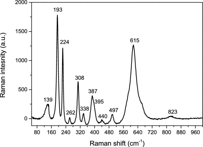
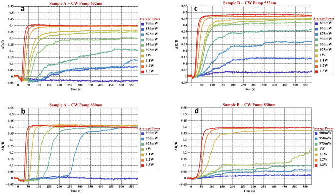
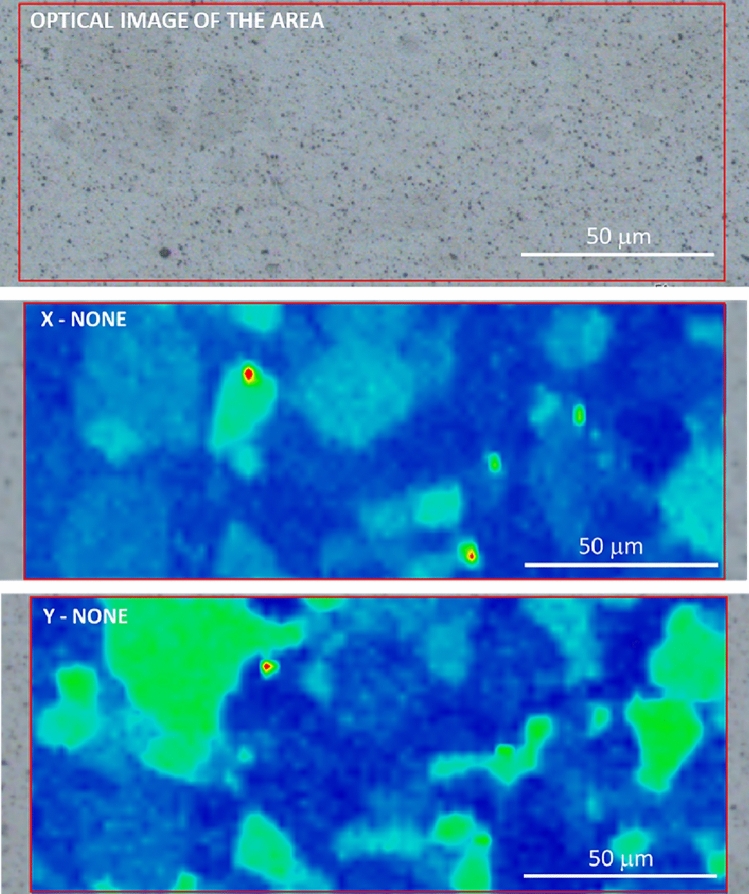
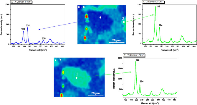
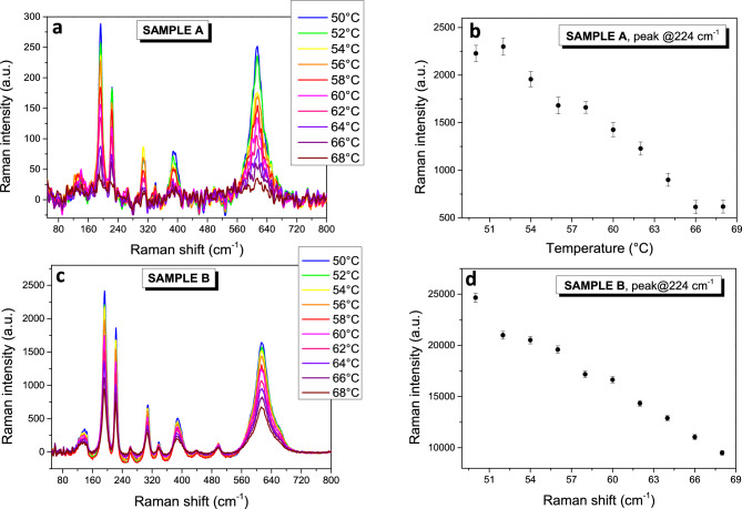
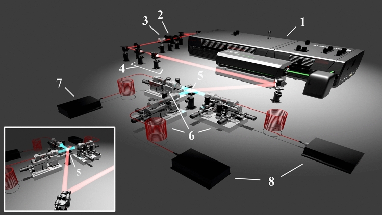
Vanadium dioxide has attracted much interest due to the drastic change of the electrical and optical properties it exhibits during the transition from the semiconductor state to the metallic state, which takes place at a critical temperature of about 68 °C. Much study has been especially devoted to developing advanced fabrication methodologies to improve the performance of VO thin films for phase-change applications in optical devices. Films structural and morphological characterisation is normally performed with expensive and time consuming equipment, as x-ray diffractometers, electron microscopes and atomic force microscopes. Here we propose a purely optical approach which combines Polarized Raman Mapping and Phase-Transition by Continuous Wave Optical Excitation (PTCWE) to acquire through two simple measurements structural, morphological and thermal behaviour information on polycrystalline VO thin films. The combination of the two techniques allows to reconstruct a complete picture of the properties of the films in a fast and effective manner, and also to unveil an interesting stepped appearance of the hysteresis cycles probably induced by the progressive stabilization of rutile metallic domains embedded in the semiconducting monoclinic matrix.
二氧化钒因其在从半导体状态转变为金属状态过程中所展现出的电学和光学性质的急剧变化而备受关注,这种转变发生在约68°C的临界温度下。大量研究尤其致力于开发先进的制造方法,以改善用于光学器件相变应用的VO薄膜的性能。薄膜的结构和形态表征通常使用昂贵且耗时的设备,如X射线衍射仪、电子显微镜和原子力显微镜。在此,我们提出一种纯光学方法,该方法结合了偏振拉曼映射和连续波光激发相变(PTCWE),通过两个简单测量来获取多晶VO薄膜的结构、形态和热行为信息。这两种技术的结合能够以快速有效的方式重建薄膜性质的完整图景,还能揭示出滞后循环中一种有趣的阶梯状外观,这可能是由嵌入半导体单斜基质中的金红石金属域的逐渐稳定所导致的。