• 文献检索
  • 文档翻译
  • 深度研究
  • 学术资讯
  • Suppr Zotero 插件Zotero 插件
  • 邀请有礼
  • 套餐&价格
  • 历史记录
应用&插件
Suppr Zotero 插件Zotero 插件浏览器插件Mac 客户端Windows 客户端微信小程序
定价
高级版会员购买积分包购买API积分包
服务
文献检索文档翻译深度研究API 文档MCP 服务
关于我们
关于 Suppr公司介绍联系我们用户协议隐私条款
关注我们

Suppr 超能文献

核心技术专利:CN118964589B侵权必究
粤ICP备2023148730 号-1Suppr @ 2026

文献检索

告别复杂PubMed语法,用中文像聊天一样搜索,搜遍4000万医学文献。AI智能推荐,让科研检索更轻松。

立即免费搜索

文件翻译

保留排版,准确专业,支持PDF/Word/PPT等文件格式,支持 12+语言互译。

免费翻译文档

深度研究

AI帮你快速写综述,25分钟生成高质量综述,智能提取关键信息,辅助科研写作。

立即免费体验

硅基氮化镓外延片中位错密度计算方法的比较研究

A Comparative Study of Methods for Calculating the Dislocation Density in GaN-on-Si Epitaxial Wafers.

作者信息

Yan Yujie, Huang Jun, Pan Lei, Meng Biao, Wei Qiangmin, Yang Bing

机构信息

JFS Laboratory, Wuhan 430074, China.

出版信息

Micromachines (Basel). 2024 Jul 25;15(8):954. doi: 10.3390/mi15080954.

DOI:10.3390/mi15080954
PMID:39203605
原文链接:https://pmc.ncbi.nlm.nih.gov/articles/PMC11356259/
Abstract

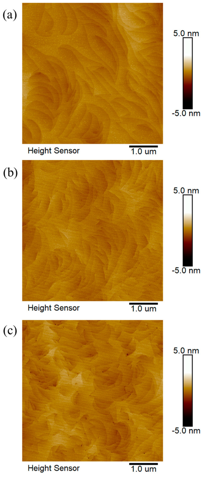
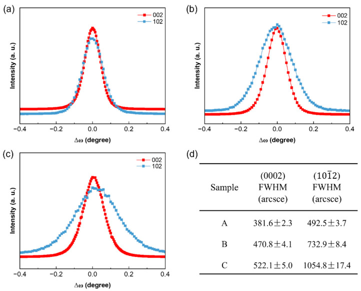
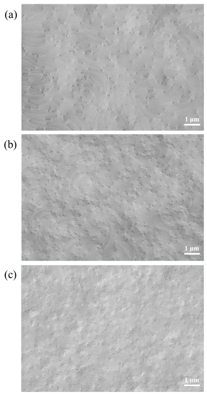
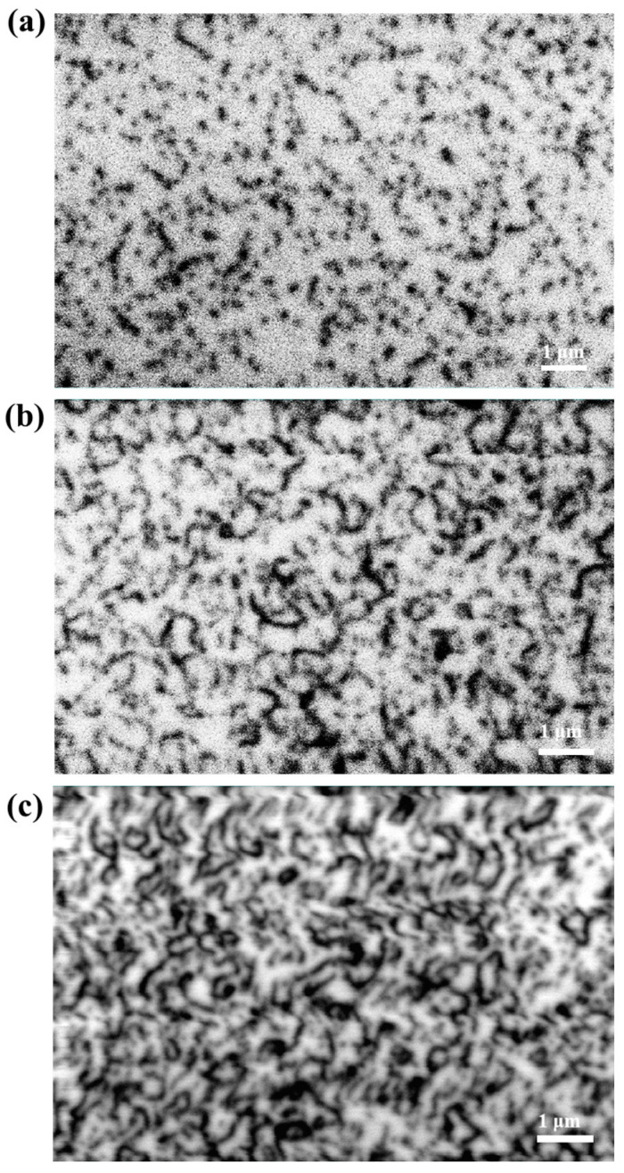
A series of characterization methods involving high-resolution X-ray diffraction (HR-XRD), electron channel contrast imaging (ECCI), cathodoluminescence microscopy (CL), and atomic force microscopy (AFM) were applied to calculate the dislocation density of GaN-on-Si epitaxial wafers, and their performance was analyzed and evaluated. The ECCI technique, owing to its high lateral resolution, reveals dislocation distributions on material surfaces, which can visually characterize the dislocation density. While the CL technique is effective for low-density dislocations, it is difficult to accurately identify the number of dislocation clusters in CL images as the density increases. The AFM technique analyzes surface dislocation characteristics by detecting surface pits caused by dislocations, which are easily affected by sample and probe conditions. A prevalent method for assessing the crystal quality of GaN is the rocking curve of HR-XRD (ω-scan), which calculates the dislocation density based on the FWHM value of the curves. By comparing the above four dislocation characterization methods, the advantages and limitations of each method are clarified, which also verifies the applicability of DB=β29b2 for GaN-on-Si epitaxial wafers. This provides an important reference value for dislocation characterization in GaN-on-Si materials. The accuracy evaluation of dislocation density can truly and reliably reflect crystal quality, which is conducive to further optimization. Furthermore, this study can also be applied to other heterogeneous or homogeneous epitaxial materials.

摘要

一系列表征方法,包括高分辨率X射线衍射(HR-XRD)、电子通道对比成像(ECCI)、阴极发光显微镜(CL)和原子力显微镜(AFM),被用于计算硅基氮化镓外延片的位错密度,并对其性能进行分析和评估。ECCI技术由于其高横向分辨率,可揭示材料表面的位错分布,能够直观地表征位错密度。虽然CL技术对低密度位错有效,但随着密度增加,在CL图像中难以准确识别位错簇的数量。AFM技术通过检测由位错引起的表面坑来分析表面位错特征,这很容易受到样品和探针条件的影响。评估氮化镓晶体质量的一种常用方法是HR-XRD的摇摆曲线(ω扫描),它根据曲线的半高宽值计算位错密度。通过比较上述四种位错表征方法,阐明了每种方法的优缺点,这也验证了DB=β29b2对硅基氮化镓外延片的适用性。这为硅基氮化镓材料中的位错表征提供了重要的参考价值。位错密度的准确性评估能够真实可靠地反映晶体质量,有利于进一步优化。此外,本研究也可应用于其他异质或同质外延材料。

https://cdn.ncbi.nlm.nih.gov/pmc/blobs/1111/11356259/0489105bf4c8/micromachines-15-00954-g005.jpg
https://cdn.ncbi.nlm.nih.gov/pmc/blobs/1111/11356259/7c60f4f8f746/micromachines-15-00954-g001.jpg
https://cdn.ncbi.nlm.nih.gov/pmc/blobs/1111/11356259/29095d49e312/micromachines-15-00954-g002.jpg
https://cdn.ncbi.nlm.nih.gov/pmc/blobs/1111/11356259/4ce2124f2d05/micromachines-15-00954-g003.jpg
https://cdn.ncbi.nlm.nih.gov/pmc/blobs/1111/11356259/724596cc0f67/micromachines-15-00954-g004.jpg
https://cdn.ncbi.nlm.nih.gov/pmc/blobs/1111/11356259/0489105bf4c8/micromachines-15-00954-g005.jpg

相似文献

1
A Comparative Study of Methods for Calculating the Dislocation Density in GaN-on-Si Epitaxial Wafers.硅基氮化镓外延片中位错密度计算方法的比较研究
Micromachines (Basel). 2024 Jul 25;15(8):954. doi: 10.3390/mi15080954.
2
Studies of Defect Structure in Epitaxial AlN/GaN Films Grown on (111) 3C-SiC.在(111) 3C - SiC上生长的外延AlN/GaN薄膜中的缺陷结构研究。
Nanomaterials (Basel). 2021 May 14;11(5):1299. doi: 10.3390/nano11051299.
3
A partly-contacted epitaxial lateral overgrowth method applied to GaN material.应用于 GaN 材料的部分接触外延横向过生长法。
Sci Rep. 2016 Apr 1;6:23842. doi: 10.1038/srep23842.
4
Dislocation characterization in-plane GaN epitaxial layers on 6 inch Si wafer with a fast second-harmonic generation intensity mapping technique.
Nanotechnology. 2023 Feb 3;34(15). doi: 10.1088/1361-6528/acb4a0.
5
Defect Structure Determination of GaN Films in GaN/AlN/Si Heterostructures by HR-TEM, XRD, and Slow Positrons Experiments.通过高分辨率透射电子显微镜、X射线衍射和慢正电子实验确定GaN/AlN/Si异质结构中GaN薄膜的缺陷结构
Nanomaterials (Basel). 2020 Jan 23;10(2):197. doi: 10.3390/nano10020197.
6
A new approach to epitaxially grow high-quality GaN films on Si substrates: the combination of MBE and PLD.一种在硅衬底上外延生长高质量氮化镓薄膜的新方法:分子束外延与脉冲激光沉积的结合。
Sci Rep. 2016 Apr 22;6:24448. doi: 10.1038/srep24448.
7
Development and analysis of thick GaN drift layers on 200 mm CTE-matched substrate for vertical device processing.用于垂直器件工艺的200毫米CTE匹配衬底上厚氮化镓漂移层的开发与分析。
Sci Rep. 2023 Sep 23;13(1):15931. doi: 10.1038/s41598-023-42747-1.
8
Selective-area growth of GaN nanocolumns on Si(111) substrates for application to nanocolumn emitters with systematic analysis of dislocation filtering effect of nanocolumns.在Si(111)衬底上选择性区域生长用于纳米柱发射器的GaN纳米柱,并对纳米柱的位错过滤效应进行系统分析。
Nanotechnology. 2015 Jun 5;26(22):225602. doi: 10.1088/0957-4484/26/22/225602. Epub 2015 May 12.
9
Screw dislocation-driven epitaxial solution growth of ZnO nanowires seeded by dislocations in GaN substrates.在 GaN 衬底中螺位错驱动的 ZnO 纳米线的外延溶液生长,这些纳米线由位错作为晶种。
Nano Lett. 2010 Sep 8;10(9):3459-63. doi: 10.1021/nl1015409.
10
Integration of GaN and Diamond Using Epitaxial Lateral Overgrowth.利用外延横向生长实现氮化镓与金刚石的集成。
ACS Appl Mater Interfaces. 2020 Sep 2;12(35):39397-39404. doi: 10.1021/acsami.0c10065. Epub 2020 Aug 20.

本文引用的文献

1
A review on the GaN-on-Si power electronic devices.关于硅基氮化镓功率电子器件的综述。
Fundam Res. 2021 Dec 8;2(3):462-475. doi: 10.1016/j.fmre.2021.11.028. eCollection 2022 May.
2
A Brief Overview of the Rapid Progress and Proposed Improvements in Gallium Nitride Epitaxy and Process for Third-Generation Semiconductors with Wide Bandgap.氮化镓外延生长及第三代宽禁带半导体工艺的快速进展与改进建议概述
Micromachines (Basel). 2023 Mar 29;14(4):764. doi: 10.3390/mi14040764.
3
Challenges and Opportunities for High-Power and High-Frequency AlGaN/GaN High-Electron-Mobility Transistor (HEMT) Applications: A Review.
高功率和高频氮化铝镓/氮化镓高电子迁移率晶体管(HEMT)应用面临的挑战与机遇:综述
Micromachines (Basel). 2022 Dec 1;13(12):2133. doi: 10.3390/mi13122133.
4
Development of GaN HEMTs Fabricated on Silicon, Silicon-on-Insulator, and Engineered Substrates and the Heterogeneous Integration.基于硅、绝缘体上硅及工程衬底制造的氮化镓高电子迁移率晶体管的发展及异质集成。
Micromachines (Basel). 2021 Sep 27;12(10):1159. doi: 10.3390/mi12101159.
5
The Evolution of Manufacturing Technology for GaN Electronic Devices.氮化镓电子器件制造技术的发展
Micromachines (Basel). 2021 Jun 23;12(7):737. doi: 10.3390/mi12070737.
6
Exploring an Approach toward the Intrinsic Limits of GaN Electronics.探索氮化镓电子学固有极限的方法。
ACS Appl Mater Interfaces. 2020 Mar 18;12(11):12949-12954. doi: 10.1021/acsami.9b19697. Epub 2020 Mar 5.