• 文献检索
  • 文档翻译
  • 深度研究
  • 学术资讯
  • Suppr Zotero 插件Zotero 插件
  • 邀请有礼
  • 套餐&价格
  • 历史记录
应用&插件
Suppr Zotero 插件Zotero 插件浏览器插件Mac 客户端Windows 客户端微信小程序
定价
高级版会员购买积分包购买API积分包
服务
文献检索文档翻译深度研究API 文档MCP 服务
关于我们
关于 Suppr公司介绍联系我们用户协议隐私条款
关注我们

Suppr 超能文献

核心技术专利:CN118964589B侵权必究
粤ICP备2023148730 号-1Suppr @ 2026

文献检索

告别复杂PubMed语法,用中文像聊天一样搜索,搜遍4000万医学文献。AI智能推荐,让科研检索更轻松。

立即免费搜索

文件翻译

保留排版,准确专业,支持PDF/Word/PPT等文件格式,支持 12+语言互译。

免费翻译文档

深度研究

AI帮你快速写综述,25分钟生成高质量综述,智能提取关键信息,辅助科研写作。

立即免费体验

氮化镓电子器件制造技术的发展

The Evolution of Manufacturing Technology for GaN Electronic Devices.

作者信息

Liu An-Chen, Tu Po-Tsung, Langpoklakpam Catherine, Huang Yu-Wen, Chang Ya-Ting, Tzou An-Jye, Hsu Lung-Hsing, Lin Chun-Hsiung, Kuo Hao-Chung, Chang Edward Yi

机构信息

Department of Photonics, Institute of Electro-Optical Engineering, National Yang Ming Chiao Tung University, Hsinchu 30010, Taiwan.

Industrial Technology Research Institute, No. 195, Sec. 4, Chung Hsing Rd., Chutung, Hsinchu 31040, Taiwan.

出版信息

Micromachines (Basel). 2021 Jun 23;12(7):737. doi: 10.3390/mi12070737.

DOI:10.3390/mi12070737
PMID:34201620
原文链接:https://pmc.ncbi.nlm.nih.gov/articles/PMC8305582/
Abstract

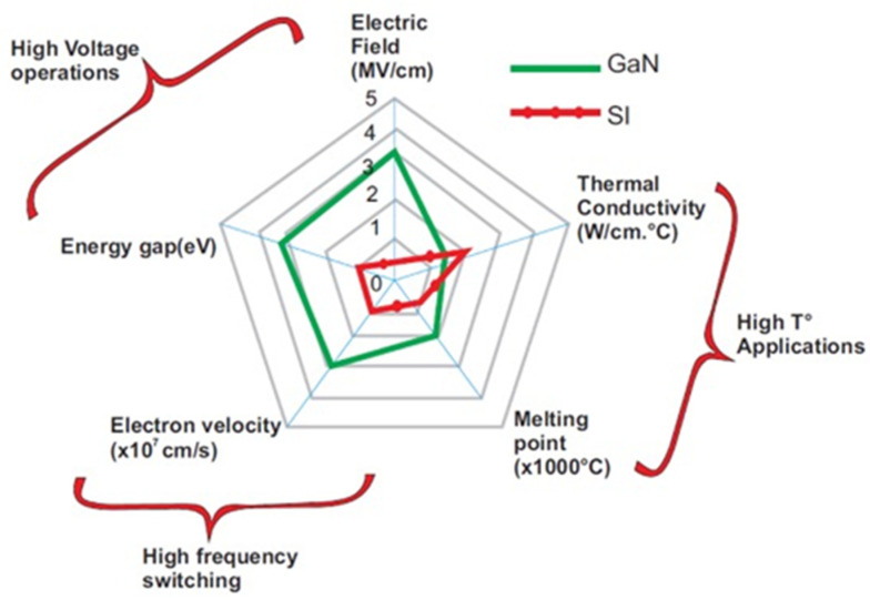
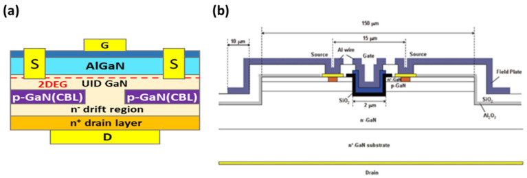
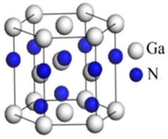
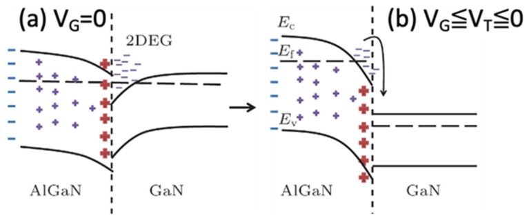
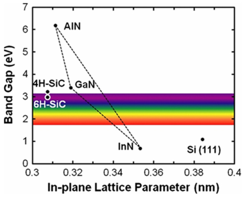
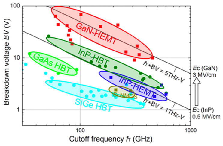
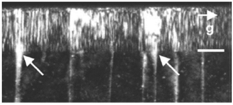
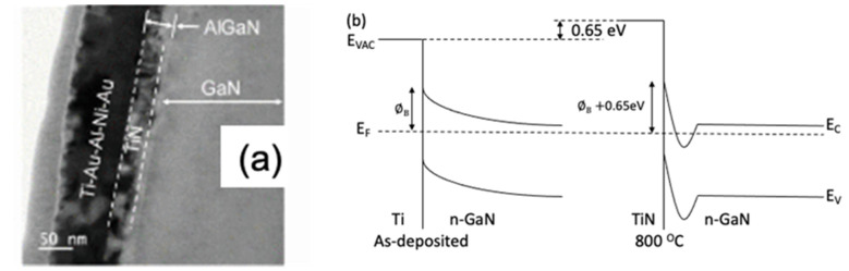
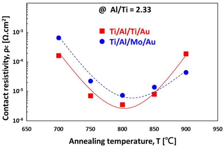
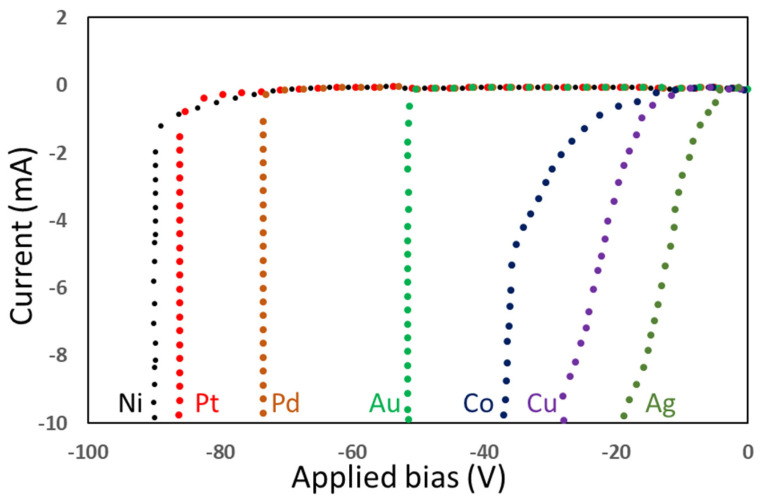
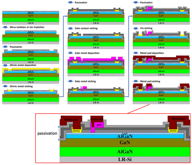
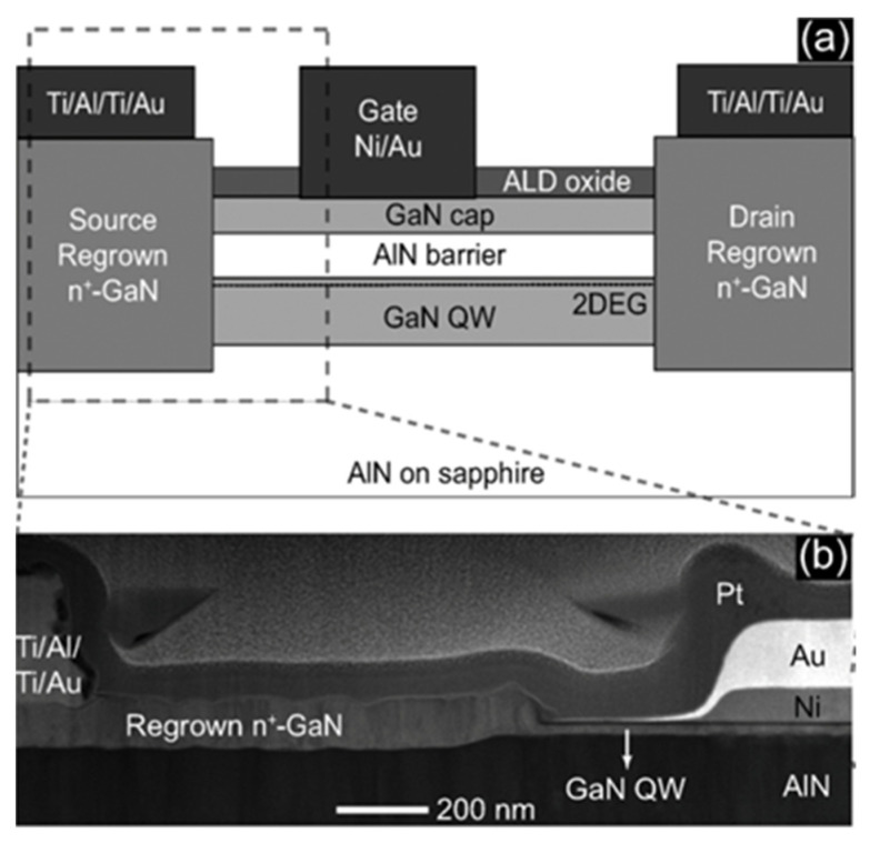
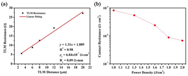
GaN has been widely used to develop devices for high-power and high-frequency applications owing to its higher breakdown voltage and high electron saturation velocity. The GaN HEMT radio frequency (RF) power amplifier is the first commercialized product which is fabricated using the conventional Au-based III-V device manufacturing process. In recent years, owing to the increased applications in power electronics, and expanded applications in RF and millimeter-wave (mmW) power amplifiers for 5G mobile communications, the development of high-volume production techniques derived from CMOS technology for GaN electronic devices has become highly demanded. In this article, we will review the history and principles of each unit process for conventional HEMT technology with Au-based metallization schemes, including epitaxy, ohmic contact, and Schottky metal gate technology. The evolution and status of CMOS-compatible Au-less process technology will then be described and discussed. In particular, novel process techniques such as regrown ohmic layers and metal-insulator-semiconductor (MIS) gates are illustrated. New enhancement-mode device technology based on the p-GaN gate is also reviewed. The vertical GaN device is a new direction of development for devices used in high-power applications, and we will also highlight the key features of such kind of device technology.

摘要

由于氮化镓(GaN)具有更高的击穿电压和高电子饱和速度,它已被广泛用于开发高功率和高频应用的器件。GaN高电子迁移率晶体管(HEMT)射频(RF)功率放大器是首个采用传统基于金的III-V族器件制造工艺制造的商业化产品。近年来,由于在电力电子领域的应用增加,以及在用于5G移动通信的射频和毫米波(mmW)功率放大器中的应用扩展,源自CMOS技术的用于GaN电子器件的大批量生产技术的开发需求大增。在本文中,我们将回顾采用基于金的金属化方案的传统HEMT技术的每个单元工艺的历史和原理,包括外延、欧姆接触和肖特基金属栅技术。然后将描述和讨论CMOS兼容的无金工艺技术的发展和现状。特别地,将说明诸如再生长欧姆层和金属-绝缘体-半导体(MIS)栅等新颖工艺技术。还将回顾基于p-GaN栅的新型增强型器件技术。垂直GaN器件是高功率应用器件的一个新的发展方向,我们也将突出此类器件技术的关键特性。

https://cdn.ncbi.nlm.nih.gov/pmc/blobs/d5d3/8305582/a9cb588c448f/micromachines-12-00737-g020.jpg
https://cdn.ncbi.nlm.nih.gov/pmc/blobs/d5d3/8305582/3e08d9d2dc02/micromachines-12-00737-g001.jpg
https://cdn.ncbi.nlm.nih.gov/pmc/blobs/d5d3/8305582/59fb194d9f17/micromachines-12-00737-g002.jpg
https://cdn.ncbi.nlm.nih.gov/pmc/blobs/d5d3/8305582/5b7ffc7bd9b0/micromachines-12-00737-g003.jpg
https://cdn.ncbi.nlm.nih.gov/pmc/blobs/d5d3/8305582/d57227caa59f/micromachines-12-00737-g004.jpg
https://cdn.ncbi.nlm.nih.gov/pmc/blobs/d5d3/8305582/39ca3784ae86/micromachines-12-00737-g005.jpg
https://cdn.ncbi.nlm.nih.gov/pmc/blobs/d5d3/8305582/b21ad7921726/micromachines-12-00737-g006.jpg
https://cdn.ncbi.nlm.nih.gov/pmc/blobs/d5d3/8305582/b6524f92aeae/micromachines-12-00737-g007.jpg
https://cdn.ncbi.nlm.nih.gov/pmc/blobs/d5d3/8305582/94bf0aceaed6/micromachines-12-00737-g008.jpg
https://cdn.ncbi.nlm.nih.gov/pmc/blobs/d5d3/8305582/86723f86df7c/micromachines-12-00737-g009.jpg
https://cdn.ncbi.nlm.nih.gov/pmc/blobs/d5d3/8305582/584a483ee616/micromachines-12-00737-g010.jpg
https://cdn.ncbi.nlm.nih.gov/pmc/blobs/d5d3/8305582/91a7c85f091a/micromachines-12-00737-g011.jpg
https://cdn.ncbi.nlm.nih.gov/pmc/blobs/d5d3/8305582/6abb869d5107/micromachines-12-00737-g012.jpg
https://cdn.ncbi.nlm.nih.gov/pmc/blobs/d5d3/8305582/699b201df9c1/micromachines-12-00737-g013.jpg
https://cdn.ncbi.nlm.nih.gov/pmc/blobs/d5d3/8305582/1c757abc5409/micromachines-12-00737-g014.jpg
https://cdn.ncbi.nlm.nih.gov/pmc/blobs/d5d3/8305582/ed5b57ddbc90/micromachines-12-00737-g015.jpg
https://cdn.ncbi.nlm.nih.gov/pmc/blobs/d5d3/8305582/fa0366df72e8/micromachines-12-00737-g016.jpg
https://cdn.ncbi.nlm.nih.gov/pmc/blobs/d5d3/8305582/c4154aeae0e9/micromachines-12-00737-g017.jpg
https://cdn.ncbi.nlm.nih.gov/pmc/blobs/d5d3/8305582/4bc492536e68/micromachines-12-00737-g018.jpg
https://cdn.ncbi.nlm.nih.gov/pmc/blobs/d5d3/8305582/013ee96638f6/micromachines-12-00737-g019.jpg
https://cdn.ncbi.nlm.nih.gov/pmc/blobs/d5d3/8305582/a9cb588c448f/micromachines-12-00737-g020.jpg

相似文献

1
The Evolution of Manufacturing Technology for GaN Electronic Devices.氮化镓电子器件制造技术的发展
Micromachines (Basel). 2021 Jun 23;12(7):737. doi: 10.3390/mi12070737.
2
Development of GaN HEMTs Fabricated on Silicon, Silicon-on-Insulator, and Engineered Substrates and the Heterogeneous Integration.基于硅、绝缘体上硅及工程衬底制造的氮化镓高电子迁移率晶体管的发展及异质集成。
Micromachines (Basel). 2021 Sep 27;12(10):1159. doi: 10.3390/mi12101159.
3
Thermal property evaluation of a 2.5D integration method with device level microchannel direct cooling for a high-power GaN HEMT device.用于高功率氮化镓高电子迁移率晶体管器件的具有器件级微通道直接冷却的2.5D集成方法的热性能评估
Microsyst Nanoeng. 2022 Nov 11;8:119. doi: 10.1038/s41378-022-00462-3. eCollection 2022.
4
Normally-Off p-GaN Gated AlGaN/GaN MIS-HEMTs with ALD-Grown AlO/AlN Composite Gate Insulator.具有ALD生长的AlO/AlN复合栅极绝缘体的常关型p-GaN栅控AlGaN/GaN MIS-HEMT
Membranes (Basel). 2021 Sep 23;11(10):727. doi: 10.3390/membranes11100727.
5
Status of Aluminum Oxide Gate Dielectric Technology for Insulated-Gate GaN-Based Devices.用于基于氮化镓的绝缘栅器件的氧化铝栅极电介质技术现状
Materials (Basel). 2022 Jan 21;15(3):791. doi: 10.3390/ma15030791.
6
GaN-based complementary inverter logic gate using InGaN/GaN superlattice capped enhancement-mode field-effect-transistors.基于氮化镓的互补反相器逻辑门,采用氮化铟镓/氮化镓超晶格覆盖增强型场效应晶体管。
Nanotechnology. 2021 May 12;32(31). doi: 10.1088/1361-6528/abfb99.
7
An Overview of Normally-Off GaN-Based High Electron Mobility Transistors.基于氮化镓的常关型高电子迁移率晶体管概述。
Materials (Basel). 2019 May 15;12(10):1599. doi: 10.3390/ma12101599.
8
Review on Main Gate Characteristics of P-Type GaN Gate High-Electron-Mobility Transistors.P型氮化镓栅极高电子迁移率晶体管的栅极特性综述
Micromachines (Basel). 2023 Dec 30;15(1):80. doi: 10.3390/mi15010080.
9
Recessed-Gate GaN Metal-Insulator-Semiconductor High-Electron-Mobility Transistor Using a Dual Gate-Insulator Employing TiO₂/SiN.采用TiO₂/SiN双栅绝缘体的凹槽栅氮化镓金属绝缘体半导体高电子迁移率晶体管
J Nanosci Nanotechnol. 2020 Aug 1;20(8):4678-4683. doi: 10.1166/jnn.2020.17809.
10
A review on the GaN-on-Si power electronic devices.关于硅基氮化镓功率电子器件的综述。
Fundam Res. 2021 Dec 8;2(3):462-475. doi: 10.1016/j.fmre.2021.11.028. eCollection 2022 May.

引用本文的文献

1
Properties Investigation and Damage Analysis of GaN Photoconductive Semiconductor Switch Based on SiC Substrate.基于碳化硅衬底的氮化镓光电导半导体开关特性研究与损伤分析
Micromachines (Basel). 2024 Sep 24;15(10):1178. doi: 10.3390/mi15101178.
2
A Comparative Study of Methods for Calculating the Dislocation Density in GaN-on-Si Epitaxial Wafers.硅基氮化镓外延片中位错密度计算方法的比较研究
Micromachines (Basel). 2024 Jul 25;15(8):954. doi: 10.3390/mi15080954.
3
Decomposition of the anisotropic strain in 3D-structure GaN layers using Raman spectroscopy.

本文引用的文献

1
Gallium Nitride (GaN) High-Electron-Mobility Transistors with Thick Copper Metallization Featuring a Power Density of 8.2 W/mm for Ka-Band Applications.用于Ka波段应用的具有厚铜金属化层、功率密度为8.2W/mm的氮化镓(GaN)高电子迁移率晶体管。
Micromachines (Basel). 2020 Feb 21;11(2):222. doi: 10.3390/mi11020222.
利用拉曼光谱法分解三维结构氮化镓层中的各向异性应变。
Sci Rep. 2024 Feb 9;14(1):3330. doi: 10.1038/s41598-024-53478-2.
4
Improvement of AlGaN/GaN HEMTs Linearity Using Etched-Fin Gate Structure for Ka Band Applications.用于Ka波段应用的采用蚀刻鳍栅结构改善AlGaN/GaN高电子迁移率晶体管的线性度
Micromachines (Basel). 2023 Apr 25;14(5):931. doi: 10.3390/mi14050931.
5
GaN Heterostructures as Innovative X-ray Imaging Sensors-Change of Paradigm.作为创新型X射线成像传感器的氮化镓异质结构——范式转变
Micromachines (Basel). 2022 Jan 19;13(2):147. doi: 10.3390/mi13020147.