Osestad Eivind Kristen, Zossimova Ekaterina, Walter Michael, Holst Bodil, Fiedler Johannes
Department of Physics and Technology, University of Bergen Allégaten 55 5007 Bergen Norway
Lace Lithography AS Allégaten 55 5007 Bergen Norway.
Nanoscale Adv. 2024 Sep 2;6(21):5337-47. doi: 10.1039/d4na00322e.
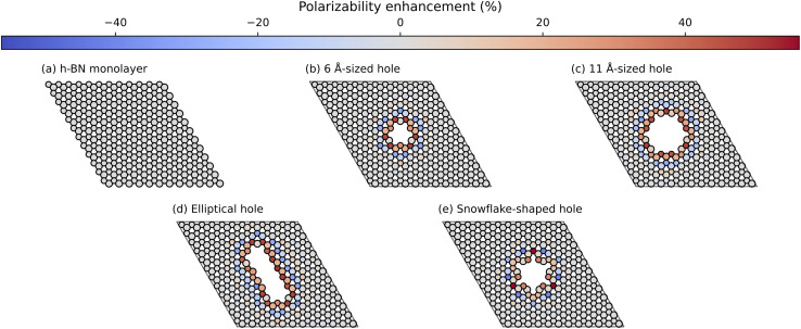
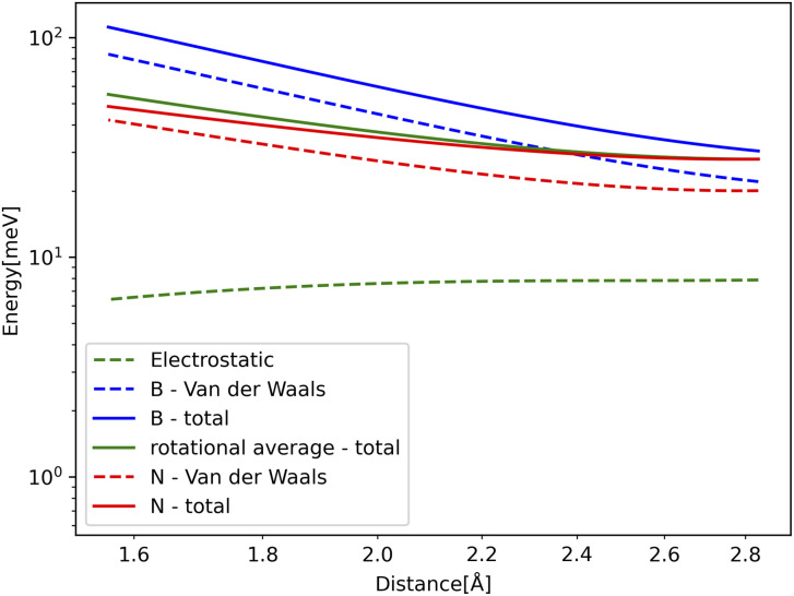
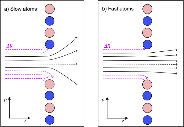
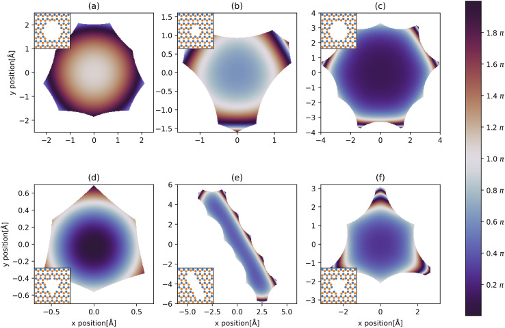
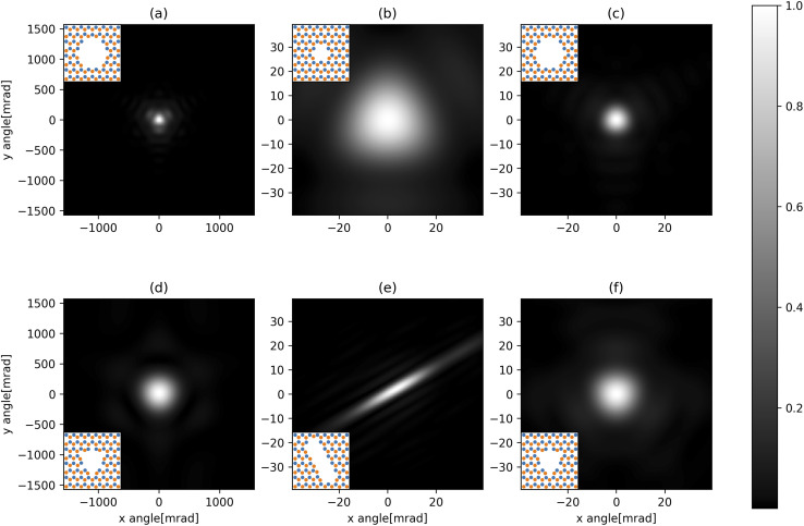
Fabricating patterned nanostructures with matter waves can help to realise new nanophotonic devices. However, due to dispersion effects, designing patterns with nanoscale features is challenging. Here, we consider the propagation of a helium matter wave through different holes in hexagonal boron nitride (h-BN) as a case study for the weakest dispersion interaction and the matter wave's diffraction as it passes through the holes. We use a quantum-mechanical model to calculate the polarisability of edge atoms around the holes, where we observe polarisation ripples of enhanced and reduced polarisabilities around the holes. We use these values to calculate van der Waals dispersion coefficients for the scattered helium atoms. We find that the resulting diffraction patterns are affected by the shape and size of the holes, where the smallest holes have a radius of just 6 Å. These results can be used to predict the resolution limits of nano-hole patterns on nanophotonic materials.
利用物质波制造图案化纳米结构有助于实现新型纳米光子器件。然而,由于色散效应,设计具有纳米级特征的图案具有挑战性。在这里,我们将氦物质波通过六方氮化硼(h-BN)中不同孔洞的传播作为最弱色散相互作用以及物质波通过孔洞时衍射的案例研究。我们使用量子力学模型来计算孔洞周围边缘原子的极化率,在那里我们观察到孔洞周围极化率增强和降低的极化波纹。我们用这些值来计算散射氦原子的范德华色散系数。我们发现,由此产生的衍射图案受孔洞形状和大小的影响,其中最小的孔洞半径仅为6埃。这些结果可用于预测纳米光子材料上纳米孔图案的分辨率极限。