Hatsuoka Ryohei, Yamasaki Kota, Wada Kenji, Matsuyama Tetsuya, Okamoto Koichi
Department of Physics and Electronics, Graduate School of Engineering, Osaka Metropolitan University, 1-1 Gakuen-cho, Naka-ku, Sakai 599-8531, Osaka, Japan.
Equipment Sharing Center for Advanced Research and Innovation, Osaka Metropolitan University, 1-1 Gakuen-cho, Naka-ku, Sakai 599-8531, Osaka, Japan.
Nanomaterials (Basel). 2024 Sep 26;14(19):1559. doi: 10.3390/nano14191559.
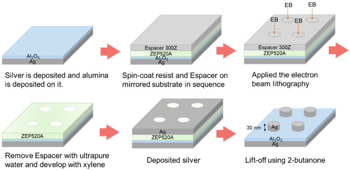
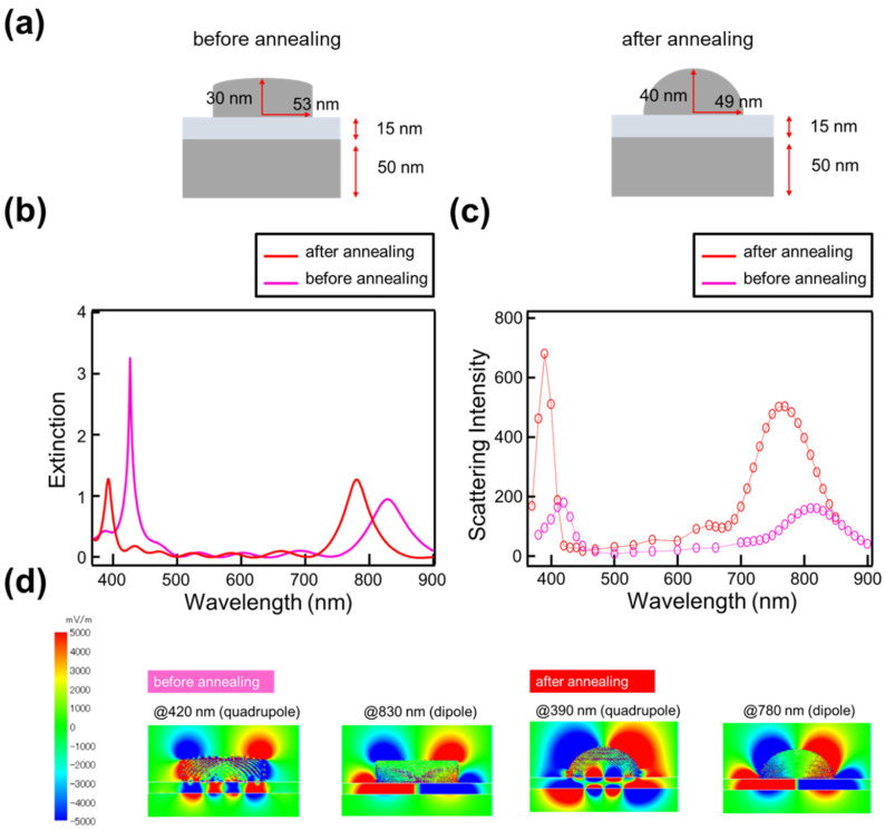
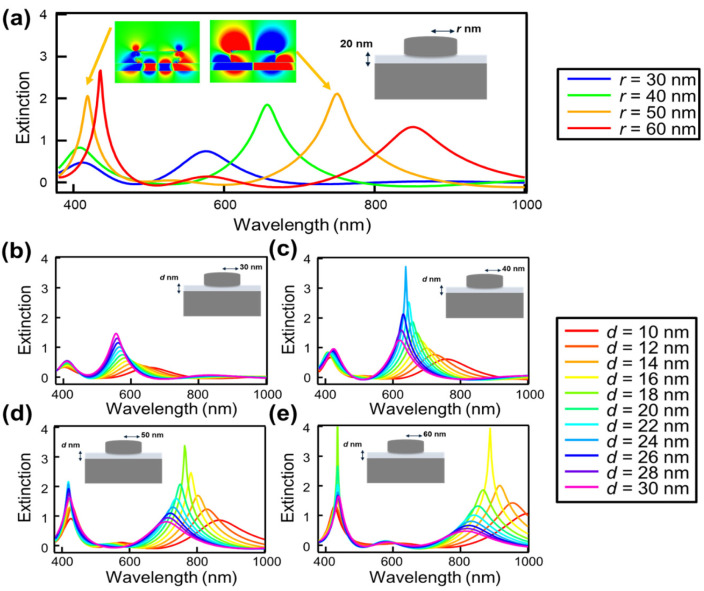
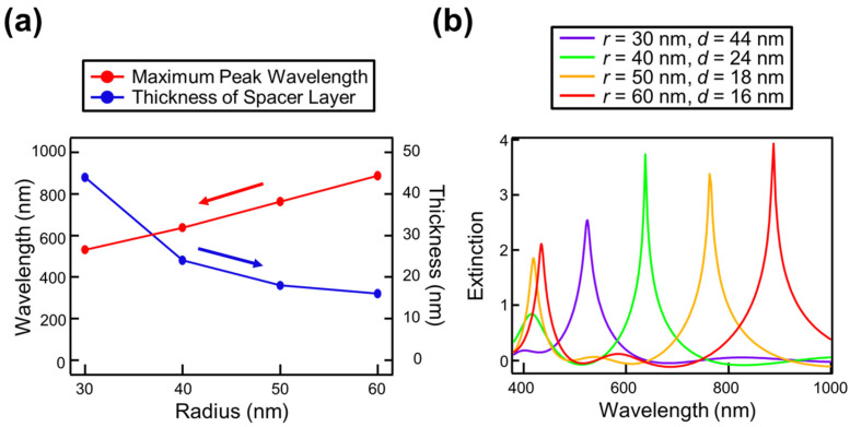
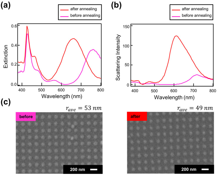
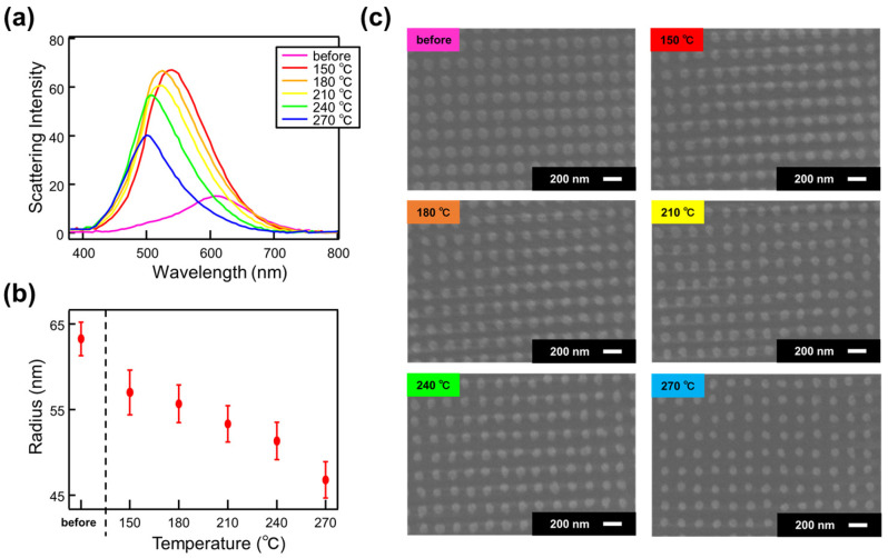
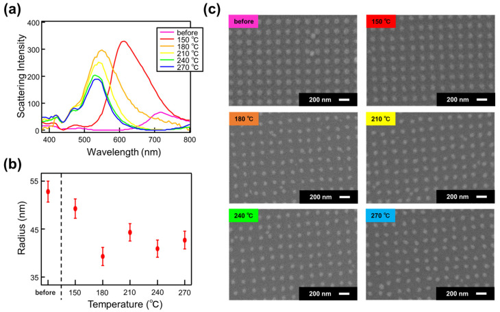
In this study, we evaluated the surface plasmon characteristics of periodic silver nanodisk structures fabricated on a dielectric thin-film spacer layer on a Ag mirror substrate (NanoDisk on Mirror: NDoM) through finite difference time domain (FDTD) simulations and experiments involving actual sample fabrication. Through FDTD simulations, it was confirmed that the NDoM structure exhibits two sharp peaks in the visible range, and by adjusting the thickness of the spacer layer and the size of the nanodisk structure, sharp peaks can be obtained across the entire visible range. Additionally, we fabricated the NDoM structure using electron beam lithography (EBL) and experimentally confirmed that the obtained peaks matched the simulation results. Furthermore, we discovered that applying annealing at an appropriate temperature to the fabricated structure enables the adjustment of the resonance peak wavelength and enhances the scattering intensity by approximately five times. This enhancement is believed to result from changes in the shape and size of the nanodisk structure, as well as a reduction in grain boundaries in the metal crystal due to annealing. These results have the potential to contribute to technological advancements in various application fields, such as optical sensing and emission enhancement.
在本研究中,我们通过时域有限差分(FDTD)模拟以及涉及实际样品制备的实验,评估了在银镜基板上的介电薄膜间隔层上制备的周期性银纳米盘结构(镜上纳米盘:NDoM)的表面等离子体特性。通过FDTD模拟,证实了NDoM结构在可见光范围内呈现出两个尖锐的峰值,并且通过调整间隔层的厚度和纳米盘结构的尺寸,可以在整个可见光范围内获得尖锐的峰值。此外,我们使用电子束光刻(EBL)制备了NDoM结构,并通过实验证实所获得的峰值与模拟结果相符。此外,我们发现对制备的结构在适当温度下进行退火能够调节共振峰波长,并将散射强度提高约五倍。这种增强被认为是由于纳米盘结构的形状和尺寸变化以及退火导致金属晶体中的晶界减少所致。这些结果有可能推动光学传感和发射增强等各种应用领域的技术进步。