Fratschko Mario, Zhao Tonghan, Fischer Jan C, Werzer Oliver, Gasser Fabian, Howard Ian A, Resel Roland
Institute of Solid State Physics, Graz University of Technology, Graz 8010, Austria.
Institute of Microstructure Technology, Karlsruhe Institute of Technology, Karlsruhe 76131, Germany.
ACS Appl Nano Mater. 2024 Nov 1;7(22):25645-25654. doi: 10.1021/acsanm.4c04763. eCollection 2024 Nov 22.
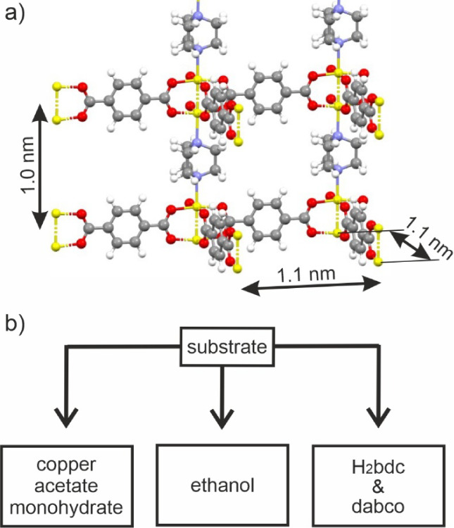
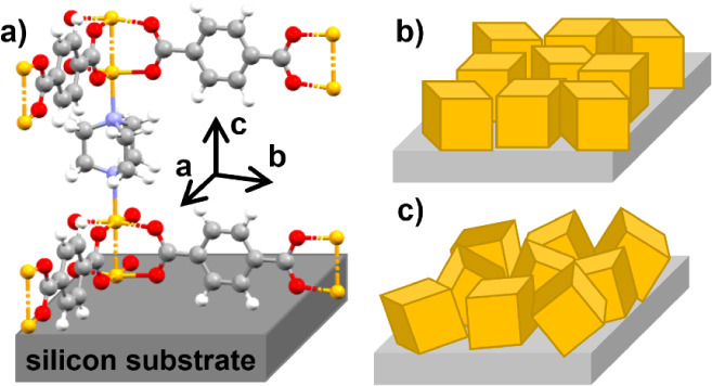
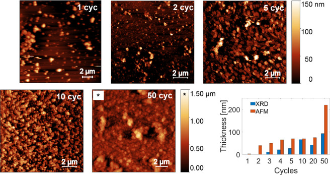
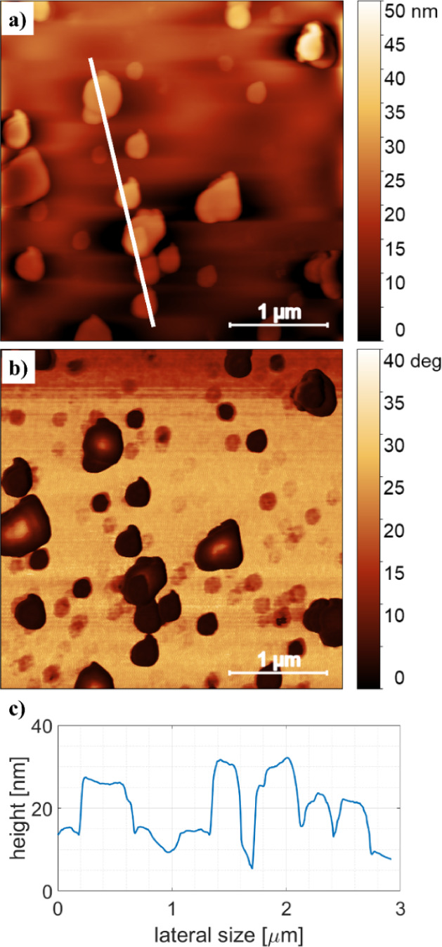
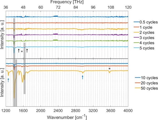
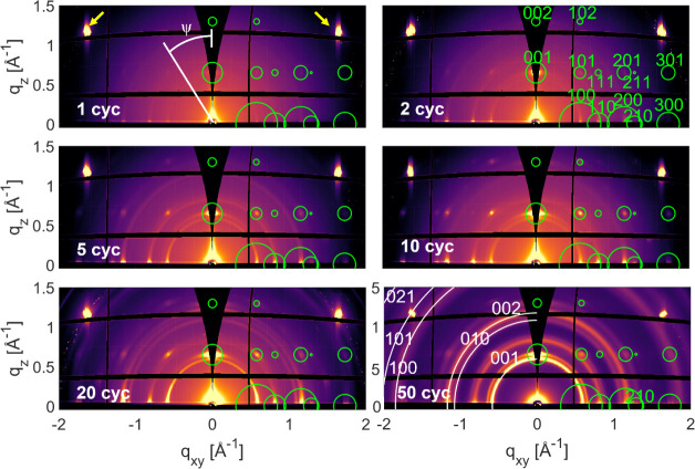
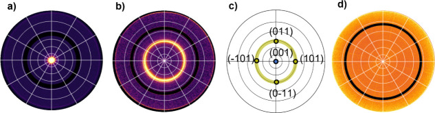
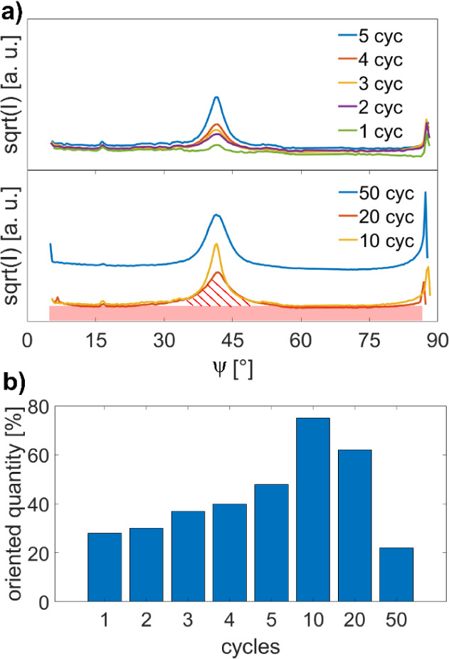
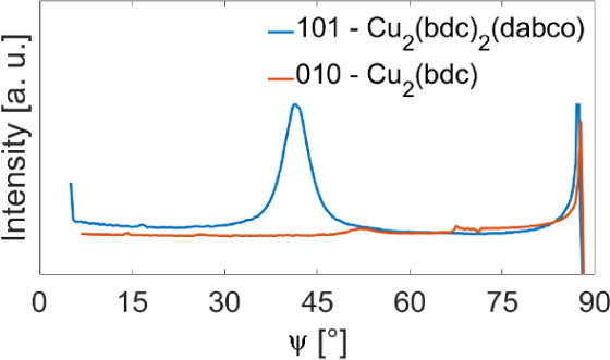
Understanding the structure of thin films is essential for successful applications of metal-organic frameworks (MOFs), such as low k-dielectrics in electronic devices. This study focuses on the thin film formation of the 3D nanoporous MOF Cu(bdc)(dabco). The thin films are prepared by a layer-by-layer technique with varying deposition cycles (1 to 50). Thin film morphologies and crystallographic properties were investigated using atomic force microscopy (AFM), Fourier transform infrared (FTIR) spectroscopy, and grazing-incidence X-ray diffraction (GIXD). AFM revealed an island growth (Volmer-Weber) with plate-like shaped islands. FTIR and GIXD revealed that Cu(bdc)(dabco) crystals form already during the first preparation cycle. The heights of the islands do not increase linearly with the number of deposition cycles, suggesting multiple growth stages. X-ray diffraction pole figures uncover a uniplanar texture of the Cu(bdc)(dabco) crystals, together with randomly oriented crystallites. The fraction of uniplanar oriented crystals increases with each deposition cycle, reaching a maximum of 75% at ten deposition cycles, simultaneously achieving complete substrate coverage. However, already at five cycles, an additional phase of randomly oriented copper-terephthalate (Cu(bdc)) crystals appeared; this phase reaches a fraction of 22% at the largest film thickness (50 cycles). In summary, a detailed understanding of the thin film formation of an archetypal layer-pillar MOF is presented, elucidating how films grow in terms of their morphology and crystalline properties. Samples prepared by ten cycles show complete coverage of the substrate together with the highest degree of preferred crystal orientation. These results establish a deepened understanding of critical parameters for MOF thin film applications, such as complete substrate coverage and definition of the nanopores relative to the substrate surface.
了解薄膜结构对于金属有机框架(MOF)的成功应用至关重要,例如电子设备中的低介电常数电介质。本研究聚焦于三维纳米多孔MOF Cu(bdc)(dabco)的薄膜形成。通过逐层技术制备薄膜,沉积循环次数不同(1至50次)。使用原子力显微镜(AFM)、傅里叶变换红外(FTIR)光谱和掠入射X射线衍射(GIXD)研究薄膜形态和晶体学性质。AFM显示出岛状生长(沃尔默-韦伯生长模式),岛呈板状。FTIR和GIXD表明,Cu(bdc)(dabco)晶体在第一个制备循环期间就已形成。岛的高度并不随沉积循环次数线性增加,这表明存在多个生长阶段。X射线衍射极图揭示了Cu(bdc)(dabco)晶体的单平面织构以及随机取向的微晶。单平面取向晶体的比例随每个沉积循环增加,在十个沉积循环时达到最大值75%,同时实现了对基底的完全覆盖。然而,在五个循环时,就出现了随机取向的对苯二甲酸铜(Cu(bdc))晶体的额外相;在最大薄膜厚度(50个循环)时,该相的比例达到22%。总之,本文详细阐述了一种典型层柱MOF的薄膜形成过程,阐明了薄膜在形态和晶体性质方面的生长方式。通过十个循环制备的样品显示出对基底的完全覆盖以及最高程度的择优晶体取向。这些结果加深了对MOF薄膜应用关键参数的理解,例如对基底的完全覆盖以及纳米孔相对于基底表面的定义。