Sittig Robert, Nawrath Cornelius, Kolatschek Sascha, Bauer Stephanie, Schaber Richard, Huang Jiasheng, Vijayan Ponraj, Pruy Pascal, Portalupi Simone Luca, Jetter Michael, Michler Peter
Institut für Halbleiteroptik und Funktionelle Grenzflächen, Center for Integrated Quantum Science and Technology (IQST) and SCoPE, University of Stuttgart, Allmandring 3, 70569 Stuttgart, Germany.
Nanophotonics. 2022 Feb 8;11(6):1109-1116. doi: 10.1515/nanoph-2021-0552. eCollection 2022 Feb.
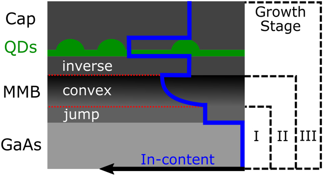
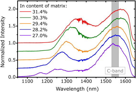
The GaAs-based material system is well-known for hosting InAs quantum dots (QDs) with outstanding optical properties, typically emitting at a wavelength of around 900 nm. The insertion of a metamorphic buffer (MMB) can shift this emission to the technologically attractive telecom C-band range centered at 1550 nm. However, the thickness of common MMB designs (>1 μm) limits their compatibility with most photonic resonator types. Here, we report on the metal-organic vapor-phase epitaxy (MOVPE) growth of a novel InGaAs MMB with a nonlinear indium content grading profile designed to maximize plastic relaxation within minimal layer thickness. This allows us to achieve the necessary transition of the lattice constant and to provide a smooth surface for QD growth within 180 nm. Single-photon emission at 1550 nm from InAs QDs deposited on top of this thin-film MMB is demonstrated. The strength of the new design is proven by integrating it into a bullseye cavity via nano-structuring techniques. The presented advances in the epitaxial growth of QD/MMB structures form the basis for the fabrication of high-quality telecom nonclassical light sources as a key component of photonic quantum technologies.
基于砷化镓的材料体系因承载具有出色光学特性的砷化铟量子点(QD)而闻名,这些量子点通常在约900纳米波长处发光。插入一个变质缓冲层(MMB)可以将这种发射波长转移到技术上具有吸引力的以1550纳米为中心的电信C波段范围。然而,常见MMB设计的厚度(>1微米)限制了它们与大多数光子谐振器类型的兼容性。在此,我们报告了一种新型铟镓砷MMB的金属有机气相外延(MOVPE)生长情况,该MMB具有非线性铟含量梯度分布,旨在在最小层厚度内最大化塑性弛豫。这使我们能够实现晶格常数的必要转变,并在180纳米内为量子点生长提供一个光滑的表面。展示了沉积在这种薄膜MMB顶部的砷化铟量子点在1550纳米处的单光子发射。通过纳米结构化技术将其集成到靶心腔中,证明了这种新设计的优势。所展示的量子点/MMB结构外延生长方面的进展为制造高质量电信非经典光源奠定了基础,而电信非经典光源是光子量子技术的关键组件。