Babich I, Reznikov I, Begichev I, Kazantsev A E, Slizovskiy S, Baranov D, Šiškins M, Zhan Z, Pantaleon P A, Trushin M, Zhao J, Grebenchuk S, Novoselov K S, Watanabe K, Taniguchi T, Fal'ko V I, Principi A, Berdyugin A I
Department of Materials Science and Engineering, National University of Singapore, Singapore, Singapore.
Institute for Functional Intelligent Materials, National University of Singapore, Singapore, Singapore.
Nat Commun. 2025 Aug 11;16(1):7389. doi: 10.1038/s41467-025-62492-5.
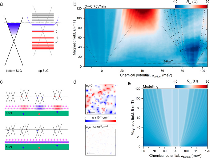
The electronic quality of graphene has improved significantly over the past two decades, revealing novel phenomena. However, even state-of-the-art devices exhibit substantial spatial charge fluctuations originating from charged defects inside the encapsulating crystals, limiting their performance. Here, we overcome this issue by assembling devices in which graphene is encapsulated by other graphene layers while remaining electronically decoupled from them via a large twist angle (~10-30°). Doping of the encapsulating graphene layer introduces strong Coulomb screening, maximized by the sub-nanometer distance between the layers, and reduces the inhomogeneity in the adjacent layer to just a few carriers per square micrometre. The enhanced quality manifests in Landau quantization emerging at magnetic fields as low as ~5 milli-Tesla and enables resolution of a small energy gap at the Dirac point. Our encapsulation approach can be extended to other two-dimensional systems, enabling further exploration of the electronic properties of ultrapure devices.
在过去二十年中,石墨烯的电学品质有了显著提升,展现出了新的现象。然而,即使是最先进的器件也存在大量源于封装晶体内部带电缺陷的空间电荷波动,这限制了它们的性能。在此,我们通过组装一种器件来克服这一问题,该器件中石墨烯被其他石墨烯层封装,同时通过大扭转角(约10 - 30°)与它们保持电学解耦。封装石墨烯层的掺杂引入了强库仑屏蔽,层间亚纳米距离使其最大化,并将相邻层中的不均匀性降低到每平方微米仅几个载流子。这种增强的品质表现为在低至约5毫特斯拉的磁场下出现朗道量子化,并能够分辨狄拉克点处的小能隙。我们的封装方法可以扩展到其他二维系统,从而能够进一步探索超纯器件的电学性质。