• 文献检索
  • 文档翻译
  • 深度研究
  • 学术资讯
  • Suppr Zotero 插件Zotero 插件
  • 邀请有礼
  • 套餐&价格
  • 历史记录
应用&插件
Suppr Zotero 插件Zotero 插件浏览器插件Mac 客户端Windows 客户端微信小程序
定价
高级版会员购买积分包购买API积分包
服务
文献检索文档翻译深度研究API 文档MCP 服务
关于我们
关于 Suppr公司介绍联系我们用户协议隐私条款
关注我们

Suppr 超能文献

核心技术专利:CN118964589B侵权必究
粤ICP备2023148730 号-1Suppr @ 2026

文献检索

告别复杂PubMed语法,用中文像聊天一样搜索,搜遍4000万医学文献。AI智能推荐,让科研检索更轻松。

立即免费搜索

文件翻译

保留排版,准确专业,支持PDF/Word/PPT等文件格式,支持 12+语言互译。

免费翻译文档

深度研究

AI帮你快速写综述,25分钟生成高质量综述,智能提取关键信息,辅助科研写作。

立即免费体验

多晶化对高介电常数电介质纳米级电学性质的影响。

Polycrystallization effects on the nanoscale electrical properties of high-k dielectrics.

作者信息

Lanza Mario, Iglesias Vanessa, Porti Marc, Nafria Montse, Aymerich Xavier

机构信息

Dept, Eng, Electrònica, Edifici Q, Campus UAB, 08193 Bellaterra, Spain.

出版信息

Nanoscale Res Lett. 2011 Jan 31;6(1):108. doi: 10.1186/1556-276X-6-108.

DOI:10.1186/1556-276X-6-108
PMID:21711617
原文链接:https://pmc.ncbi.nlm.nih.gov/articles/PMC3211152/
Abstract

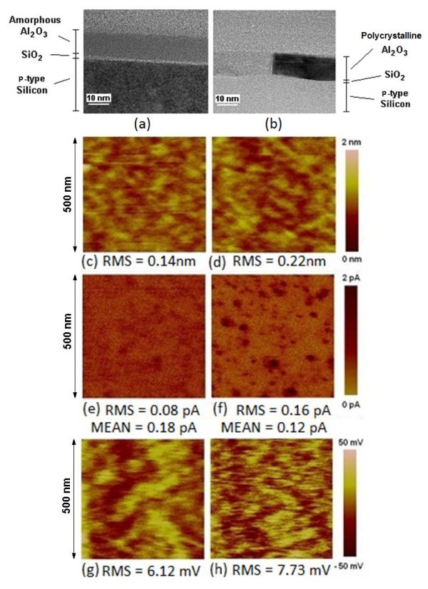
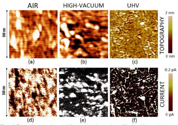
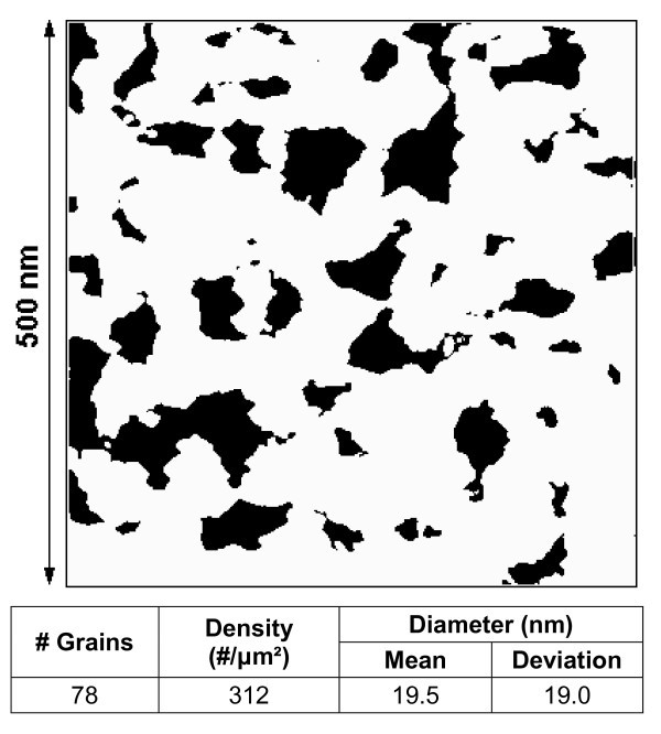
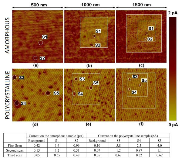
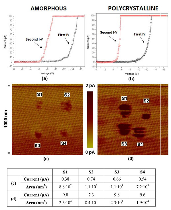
In this study, atomic force microscopy-related techniques have been used to investigate, at the nanoscale, how the polycrystallization of an Al2O3-based gate stack, after a thermal annealing process, affects the variability of its electrical properties. The impact of an electrical stress on the electrical conduction and the charge trapping of amorphous and polycrystalline Al2O3 layers have been also analyzed.

摘要

在本研究中,已使用与原子力显微镜相关的技术在纳米尺度上研究基于Al2O3的栅极堆叠在热退火过程后的多晶化如何影响其电学性质的可变性。还分析了电应力对非晶和多晶Al2O3层的导电和电荷俘获的影响。

https://cdn.ncbi.nlm.nih.gov/pmc/blobs/0eaf/3211152/b8c3c8b91009/1556-276X-6-108-5.jpg
https://cdn.ncbi.nlm.nih.gov/pmc/blobs/0eaf/3211152/b739313b3c76/1556-276X-6-108-1.jpg
https://cdn.ncbi.nlm.nih.gov/pmc/blobs/0eaf/3211152/423d0a506b17/1556-276X-6-108-2.jpg
https://cdn.ncbi.nlm.nih.gov/pmc/blobs/0eaf/3211152/8be93b352975/1556-276X-6-108-3.jpg
https://cdn.ncbi.nlm.nih.gov/pmc/blobs/0eaf/3211152/ad49a3638d1e/1556-276X-6-108-4.jpg
https://cdn.ncbi.nlm.nih.gov/pmc/blobs/0eaf/3211152/b8c3c8b91009/1556-276X-6-108-5.jpg

相似文献

1
Polycrystallization effects on the nanoscale electrical properties of high-k dielectrics.多晶化对高介电常数电介质纳米级电学性质的影响。
Nanoscale Res Lett. 2011 Jan 31;6(1):108. doi: 10.1186/1556-276X-6-108.
2
Interface Electrical Properties of AlO Thin Films on Graphene Obtained by Atomic Layer Deposition with an in Situ Seedlike Layer.原子层沉积原位种子层法制备石墨烯上 AlO 薄膜的界面电学性能
ACS Appl Mater Interfaces. 2017 Mar 1;9(8):7761-7771. doi: 10.1021/acsami.6b15190. Epub 2017 Feb 13.
3
Electronic Structure and Charge-Trapping Characteristics of the AlO-TiAlO-SiO Gate Stack for Nonvolatile Memory Applications.用于非易失性存储器应用的AlO-TiAlO-SiO栅堆叠的电子结构和电荷俘获特性
Nanoscale Res Lett. 2017 Dec;12(1):270. doi: 10.1186/s11671-017-2040-x. Epub 2017 Apr 13.
4
Interfacial Cation-Defect Charge Dipoles in Stacked TiO/AlO Gate Dielectrics.堆叠 TiO/AlO 栅介质中的界面阳离子-缺陷电荷偶极子。
ACS Appl Mater Interfaces. 2018 Feb 14;10(6):5140-5146. doi: 10.1021/acsami.7b19619. Epub 2018 Jan 30.
5
Effect of Thermal Budget on the Electrical Characterization of Atomic Layer Deposited HfSiO/TiN Gate Stack MOSCAP Structure.热预算对原子层沉积HfSiO/TiN栅堆叠MOSCAP结构电学特性的影响
PLoS One. 2016 Aug 29;11(8):e0161736. doi: 10.1371/journal.pone.0161736. eCollection 2016.
6
Atomic layer deposition of high-k dielectrics on single-walled carbon nanotubes: a Raman study.原子层沉积法在单壁碳纳米管上沉积高介电常数介质:拉曼研究。
Nanotechnology. 2013 Jun 21;24(24):245703. doi: 10.1088/0957-4484/24/24/245703. Epub 2013 May 21.
7
Modulating the interface quality and electrical properties of HfTiO/InGaAs gate stack by atomic-layer-deposition-derived Al₂O₃ passivation layer.通过原子层沉积法制备的Al₂O₃钝化层调节HfTiO/InGaAs栅堆叠的界面质量和电学性能。
ACS Appl Mater Interfaces. 2014 Dec 24;6(24):22013-25. doi: 10.1021/am506351u. Epub 2014 Dec 15.
8
Tailoring the Electrical Properties of HfO2 MOS-Devices by Aluminum Doping.通过铝掺杂来调整 HfO2 MOS 器件的电学性能。
ACS Appl Mater Interfaces. 2015 Aug 12;7(31):17032-43. doi: 10.1021/acsami.5b03071. Epub 2015 Jul 30.
9
Radiation Tolerance and Charge Trapping Enhancement of ALD HfO/AlO Nanolaminated Dielectrics.原子层沉积HfO₂/Al₂O₃纳米层状电介质的辐射耐受性及电荷俘获增强特性
Materials (Basel). 2021 Feb 10;14(4):849. doi: 10.3390/ma14040849.
10
Silicon diffusion control in atomic-layer-deposited Al2O3/La2O3/Al2O3 gate stacks using an Al2O3 barrier layer.使用Al2O3阻挡层对原子层沉积的Al2O3/La2O3/Al2O3栅极堆叠中的硅扩散进行控制。
Nanoscale Res Lett. 2015 Mar 19;10:141. doi: 10.1186/s11671-015-0842-2. eCollection 2015.

引用本文的文献

1
Understanding Current Instabilities in Conductive Atomic Force Microscopy.理解导电原子力显微镜中的当前不稳定性。
Materials (Basel). 2019 Feb 1;12(3):459. doi: 10.3390/ma12030459.
2
A Review on Resistive Switching in High-k Dielectrics: A Nanoscale Point of View Using Conductive Atomic Force Microscope.基于导电原子力显微镜的高介电常数介质中电阻开关的纳米尺度视角综述
Materials (Basel). 2014 Mar 13;7(3):2155-2182. doi: 10.3390/ma7032155.
3
Analysis on the Filament Structure Evolution in Reset Transition of Cu/HfO2/Pt RRAM Device.

本文引用的文献

1
Note: Electrical resolution during conductive atomic force microscopy measurements under different environmental conditions and contact forces.注意:在不同环境条件和接触力下进行导电原子力显微镜测量时的电学分辨率。
Rev Sci Instrum. 2010 Oct;81(10):106110. doi: 10.1063/1.3491956.
Cu/HfO2/Pt 电阻式随机存取存储器(RRAM)器件复位转变过程中细丝结构演变的分析
Nanoscale Res Lett. 2016 Dec;11(1):269. doi: 10.1186/s11671-016-1484-8. Epub 2016 May 25.
4
A hot hole-programmed and low-temperature-formed SONOS flash memory.一种热孔程序化和低温成型的 SONOS 闪存。
Nanoscale Res Lett. 2013 Jul 31;8(1):340. doi: 10.1186/1556-276X-8-340.
5
Structure and electrical properties of sputtered TiO2/ZrO2 bilayer composite dielectrics upon annealing in nitrogen.溅射沉积的TiO₂/ZrO₂双层复合电介质在氮气中退火后的结构与电学性能
Nanoscale Res Lett. 2012 Jan 5;7(1):31. doi: 10.1186/1556-276X-7-31.